Can Advanced Assembly Techniques Alter the Dynamic of Display Manufacturing?
Can Advanced Assembly Techniques Alter the Dynamic of Display Manufacturing?
The mass production of flat-panel displays has been dominated by the use of TFTs, deposited via vacuum lithography, to drive LCD or OLED panels. This approach has been a strength in terms of standardization and massive scale up to Gen 10 fabs and beyond, but also a weakness in that the cost has made profitability elusive over a quarter century of production and in a limited selection of display shapes and sizes. Emerging manufacturing techniques that combine semiconductor production with relatively simple assembly have the potential to change this dynamic.
by Paul Semenza
SINCE the first TFT-LCDs went into mass production in the late 1980s, vacuum-based photolithography has been the most important part of the manufacturing process for FPDs. It is critical to the process of fabricating TFTs on increasingly larger substrates to create the backplanes for active-matrix LCDs, OLEDs, and EPDs. The ability to deposit the multiple layers (requiring as many as 10 mask steps) needed to create advanced TFTs across square meters of area has enabled larger and higher-resolution displays every year for decades. The process has also been flexible enough to enable different TFT types, including amorphous-silicon, low-temperature polysilicon, and metal oxides, which in turn have allowed faster switching and smaller devices.
However, this progress has come at great cost, with advanced TFT fabs requiring billions of dollars in capital expenditure. Once a company has invested such sums of money, the financial imperative is to keep the fab fully utilized by making high volumes of ever-larger panels, regardless of demand. This has meant that FPD manufacturing continues to be a very risky business financially. The shift in investment from TFT-LCDs to AMOLED displays has only accentuated the risk since the TFT backplanes for OLED displays are more challenging to produce (and the organic material deposition process is not nearly as mature as that for LCDs). The need to keep fabs running at full capacity has also led to a high degree of commoditization because the similar-sized fabs produce similar panel sizes because sizes are chosen to maximize the usable area of the substrate. The lack of interest in or lack of capability on the part of leading manufacturers with regard to producing non-standard panels has enabled some more specialized firms to use older fully amortized fabs to produce custom panels, but this accounts for a modest share of industry revenues.
Some believe that a shift to flexible displays – in particular, the long-held dream of roll-to-roll manufacturing of displays – will enable the production of various sizes, shapes, and types, not driven by the need to fit into a specific substrate size and not driven by the high costs of vacuum lithography. Current techniques – such as EPLAR developed by Philips and SUFTLA developed by Seiko-Epson – involve producing the TFT array on rigid carriers in a batch process, then using a laser release process to separate the array, which is then bonded to a flexible substrate. This process is currently limited to small array sizes. It is likely to be some time before flexible OLEDs (or any other equivalent in terms of performance) will be mass-produced outside of a modified batch process using vacuum deposition. (EPLAR and SUFTLA are described in the article “Lasers Enable Diverse Display Production Techniques” by Rainer Paetzel of Coherent, GmbH, in the April 2009 issue.)
Breaking Out of the TFT Trap
However, this does not necessarily mean that the FPD industry will always be shackled to the high-cost standardized-product manufacturing model, as methods
under development outside the industry could have implications for FPD manufacturing. An ongoing series of efforts has been aimed at utilizing mature wafer-based
semiconductor processes – such as CMOS transistors or processing epitaxial wafers for LEDs – then dicing the wafers into individual chips and using various techniques to assemble the devices onto a large-area substrate used for displays or lighting products.
The common element of these approaches is that they seek to de-couple the production of backplane and display, by taking advantage of the scale and low
cost of semiconductor manufacturing1 and then using relatively simple assembly techniques to distribute the circuits across the large area of a display substrate. Since the assembly techniques are largely done outside a vacuum and at room
temperatures, they can be used for plastic substrates and also in roll-to-roll processing. Also, since CMOS transistors have much higher electron mobility than TFTs, they are especially attractive as backplanes for OLED displays, given the high-current requirements, as well as for very-high-pixel-count displays, such
as 8K × 4K, given the requirement for very fast switching speeds. Some of the same advantages are seen for the use of these techniques to assemble arrays of inorganic LEDs, whether for solid-state lighting, display backlighting, or direct-view LED displays.
Pick, Place, and Assemble
In one such technique, called fluidic self-assembly, circuits are fabricated on wafers and are then shaped and removed through etching into “nanoblocks,” which can range in size from 10 to several hundred microns. The nanoblocks are then suspended in a liquid and flowed onto a substrate into which cavities of appropriate size and shape have been etched, stamped, molded, or laser drilled. Fluidic self-assembly was developed at the University of California at Berkeley
in the 1990s and proposed for assembly of LED arrays as well as TFT backplanes. Alien Technology was formed to pursue applications in flat-panel displays, but
the technology was never successfully demonstrated for display production, and Alien moved to focus on RFIDs. (Information Display ran an article on this flat-panel research, “Bringing Alien Technology Down to Earth,” in the November 2000 issue.)
Another technique, pick and place, has been used for years in circuit-board assembly and chip packaging, although mainly for large devices and at rates too slow for assembling thousands of pixels on a display or LED array. A startup called Luxvue developed a high-throughput version of pick-and-place assembly for creation of micro-LED (devices 100 µm or smaller) arrays. The transfer device uses an arrangement of protruding mesas, each of which contains electrodes with a thin coating of dielectric. By providing a charge between the electrodes, an electrical field is created that electrostatically attracts the miniature chips. The approach enables selectively choosing to remove specific micro-devices from a source substrate by applying voltage only to the projecting mesas corresponding to the positions of the device to be transferred. This could enable the manufacture of micro-LED backlights or displays. Other than filing patents, Luxvue released very little information, and in 2014 was acquired by Apple, which has not commented on its plans for the technology.
A Different Type of Printing
In a wide-ranging effort, first at Bell Laboratories and, since 2003, at the University of Illinois at Urbana-Champaign (UIUC), John Rogers has led groups developing micro-transfer printing, a process in which a structured elastomer print-head or stamp is used to transfer microscale semiconductor devices from their native substrates onto other substrates. Rogers and colleagues have demonstrated the use of transfer printing with micro-LEDs, TFTs, carbon nanotubes, graphene, and other materials. This approach has multiple benefits, including the ability to work with different types of semiconductors and substrates; the ability to transfer large numbers of devices in parallel, and to do so in a way that translates from dense wafer arrays to sparser arrays on substrates in a precisely controllable fashion; and, finally, simplicity in that the lift-off and attach processes are conducted at room temperature and pressure, without the need for adhesives or other chemical processes.
In 2006, Semprius was spun out of UIUC to commercialize the technology. Working with Kodak before it sold its OLED business to LG Display, Semprius demonstrated the ability to create AMOLED displays using 167 × 50 × 8 mm CMOS chips that were etched and removed with an elastomer print-head and transferred onto a glass substrate.2 The company also reported producing backplanes suitable for 5-in. QVGA full-color AMOLED displays in which each IC was designed to drive two pixels (six subpixels); the array of 192 × 240 chips was transfer-printed with a process yield in excess of 99.9% and sub-micron placement accuracy.3 The printer used at the time was capable of handling up to 200-mm-diameter source wafers and target substrates up to 500 mm x 400 mm. In 2013, X-Celeprint was founded by acquiring the rights to the technology outside of photovoltaic applications.
Printing Arrays of LEDs
In 2009, Rogers and colleagues published results of work applying transfer printing to the creation of arrays of LEDs, combined with printed metal mesh for connection of the arrays, thus enabling arrays of LEDs to be constructed on metal or even plastic substrates.4 The demonstrations involved the creation of GaAs LEDs as small as 25 × 25 mm, in arrays as large as 40 × 40, deposited on glass and plastic sheets, enabling transparent displays (with less than 1% of the display area accounted for by the printed LEDs) as well as flexible and also stretchable configurations. The authors suggested that the process could be competitive with LCD and OLED panels and direct-view LED displays, as well as enabling transparent and head-up displays.
In some cases, materials that are difficult to deposit directly with the required resolution and performance may be deposited through transfer printing. For example, Samsung demonstrated quantum-dot (QD) light emission in a display through spin-coating, but was not able to pattern individual RGB QDs due to cross-contamination and found that other techniques resulted in poor quantum efficiency. However, following work at MIT,5 Samsung was able to demonstrate 4-in. full-color QD displays (driven by oxide TFTs) on glass and plastic substrates using a nano-transfer process.6
Solid-State Lighting First
The more direct path to market for this technology appears to be in solid-state lighting. In 2009, Cooledge Lighting was spun out of the UIUC work (Fig. 1).
In 2011, Rogers’ group published further work outlining materials and techniques for interconnection, thermal management, wavelength conversion, and light
distribution in thin, flexible, solid-state lighting systems created through transfer printing.7 They demonstrated white-light performance by using laminated films of YAG phosphors precisely deposited onto sparse arrays of micro-LEDs. The authors showed that the use of sparse arrays of micro-LEDs enables the use of an equivalent amount of LED dice to illuminate a large area without the need for heat sinks and special light management. In 2012, a group at the Korea Advanced Institute of Science and Technology reported transfer printing of individual GaN devices onto a polyimide substrate and also made white-light LEDs. The group suggested the possibility of flexible backlight units.8
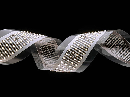
Fig. 1: This flexible LED light sheet was developed by Cooledge Lighting.
Can Printing Change Display Dynamics?
Could future display backplanes – or direct-emission displays – be produced through transfer printing or electrostatic pick and place of CMOS or epitaxial semiconductors? As has been the case with many other promising technologies, the question will largely be answered through attempts to scale up the technology to mass production. A fab that starts 60,000 sheets a month, producing 8-up full-HD panels at a 95% yield rate might create as many as 3 billion pixels an hour, which is orders of magnitude more than the capability of the systems disclosed to date. In any event, flat-panel makers are not likely to change such a crucial aspect
of their production process, even if that process results in significant swings in profitability.
While it is not likely that these assembly technologies would replace TFTs in LCDs, there could be entry points in new forms of direct-view LED displays, lighting, backlighting, transparent displays, and other non-standard display types. With very little investment, researchers have demonstrated the potential that both transfer printing and electrostatic pick and place have for accurate high-yield placement of high-performance semiconductor devices. Such displays can break out of the commodity flat-panel market – Sony caused a stir at the 2012 Consumer Electronics Show with its “Crystal LED Display,” a 55-in. full-HD direct LED display, but it was apparently so difficult to produce that the company dropped the technology. It will be interesting to see what transfer printing could do with even a fraction of the tens of billions of dollars that have been invested in TFT process equipment to date.
References
1As noted by Dan Hutcheson in IEEE Spectrum, in 2014, the semiconductor industry produced 250 billion billion (250 × 1018) transistors, at roughly a billionth of a dollar each; http://spectrum.ieee.org/computing/hardware/transistor-production-has-reached-astronomical-scales.
2C. A. Bower, E. Menard, S. Bonafede, J. W. Hamer, and R. S. Cok, “Active-Matrix OLED Backplanes using Transfer-Printed Microscale Integrated Circuits,” Proc. Elec. Comp. Tech. Conf. (60th ECTC) (2010).
3C. A. Bower, D. Gomez, K. Lucht, B. Cox, D. Kneeburg, “Transfer-Printed Integrated Circuits for Display Backplanes,” Proc. IDW ’10, 1203–1206 (2010).
4S-I. Park et. al., “Printed Assemblies of Inorganic Light-Emitting Diodes for Deformable and Semitransparent Displays,” Science 325, 977–981 (2009).
5L. Kim et al., Contact printing of quantum-dot light-emitting devices, Nano Lett. 8, 4513–4517 (2008).
6T.-H. Kim et al., “Full-colour quantum-dot displays fabricated by transfer printing,” Nature Photonics 5, 176–182 (2011).
7H. Kim et al., “Unusual Strategies for Using Indium Gallium Nitride Grown on Silicon (111) for Solid-State Lighting,” Proc. Nat. Acad. Sci. 108 (25), 10072–10077 (2011).
8H. G. Yoo et al., “Flexible GaN LED on a Polyimide Substrate for Display Applications,” Proc. SPIE 8268 (2012). •
Paul Semenza, an independent consultant, has managed market research in flat-panel displays and photovoltaics, including The NPD Group’s DisplaySearch and Solarbuzz businesses, and iSuppli’s display business. He can be reached at psemenza@gmail.com.