Ink-Jet Printing of PLED Displays
After years of materials, hardware, and process development, the ink-jet printing of polymerlight-emitting-diode displays is on the verge of becoming a practical, commercial reality.
by Jonathan Halls
FOLLOWING the first fortuitous observation of a faint green glow from a sample of a polymer material by a team at Cambridge University in 1989, Cambridge Display Technology (CDT) was founded in 1992 to develop this luminescence effect into a commercially viable emissive-display technology. Over the past 12 years, extensive work has been done by CDT and other companies to develop the performance – primarily efficiency, color, and stability – of polymer light-emitting-diode (PLED) technology to a level at which the requirements of real applications can be met.
PLEDs are a very versatile technology, which has the potential to be used for lighting, simple alphanumeric displays, and full-color flat-panel displays (FPDs). While the lifetimes of red and green devices have been acceptable for many applications for a number of years now, the much shorter lifetime of blue devices has prohibited their widespread use until recently. However, with an R&D program on blue PLEDs delivering substantial improvements in this area, and with the development of a range of new blue-emitting polymers, full-color PLED displays can now be used in a range of products. Moreover, the continual rapid progress in lifetime and stability means that more-challenging applications, such as TV, will probably be feasible in the foreseeable future.
However, in commercializing a new display technology, device performance is only one part of the story. Unless PLED displays can be manufactured in a cost-effective way in volumes high enough to satisfy the vast appetite of the display market, PLEDs will never fulfill anything other than niche applications.
One characteristic that is very interesting from a manufacturing perspective is that PLED materials are solution-processable, unlike the vacuum-deposited materials used to fabricate small-molecule-OLED displays. This brings with it a new set of challenges and opportunities. First, the coating and deposition methods used to deposit solution-processable PLEDs are scalable to large substrate sizes. In contrast, the complexity, cost, relatively low material-utilization efficiency, and mask-registration issues associated with vacuum deposition present considerable difficulties in the application of small-molecule-OLED-display production to large substrates. However, while vacuum-deposition systems are common in the display industry, coating with light-emitting-polymer (LEP) semiconductors uses processes much more familiar to the graphical printing industry.
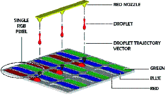
Fig. 1: In this illustration of the ink-jet-printing process as applied to PLED-display fabrication, the red-light-emitting-polymer ink is deposited into the appropriate subpixel wells, following deposition of the blue and green materials. (Courtesy of Spectra, Inc.)
This article will explore recent developments in the manufacturing techniques, plant, and infrastructure that will enable PLEDs to compete effectively with existing and other emerging display technologies. It will also try to predict when we can expect to see the first full-color PLED-display products on the market using these production technologies.
Existing Commercial Products
Up to now, the commercialization of PLEDs has occurred on a limited scale. The first volume consumer product that incorporated a PLED display was the Philips Sensotec shaver, launched in 2002, which used a small monochrome orange display with icons, fixed legends, and a small alphanumeric panel to indicate battery-charge status and main-tenance requirements. This display was manufactured in Philips's PLED-display production plant in Heerlen, The Netherlands, using a simple spin-coating process to deposit the LEP and hole-transport layers.
More recently, Philips launched the Magic Mirror 639 mobile-telephone handset with a monochrome passive-matrix secondary display behind a semi-transparent mirror that forms part of the exterior case of the clamshell telephone. Philips reports that the telephone has been selling extremely well.
OSRAM Opto Semiconductors is currently shipping a range of small monochrome (predominantly green, orange, and yellow) PLED displays manufactured at its facility in Penang, Malaysia. The displays are being sold to OEM manufacturers for inclusion in a range of electronic devices from point-of-sale displays to high-end audio-mixing desks. Delta Electronics and RiTdisplay (both located in Taiwan) are also manufacturing a range of simple passive-matrix alphanumeric and graphic displays. What all of these displays have in common is that they are monochrome, manufactured by a simple spin-coating process, and are generally from 1 to 2 in. on the diagonal.
Full-Color Ink-Jet Printing
In order to make a full-color PLED FPD, an array of individual red, green, and blue PLED subpixels must be fabricated on the display backplane. This requires red, green, and blue polymers to be deposited on specific areas of the substrate. A simple blanket deposition technique such as spin-coating is clearly not appropriate for such displays, unless a patterning technique is used to remove polymer from where it is not needed after depositing each color material. Subtractive patterning, such as the photolithographic techniques common in the silicon-semiconductor industry, is feasible with some LEP materials, but the harsh processing conditions, extra cost, and complexity of such a multi-stage approach usually rules it out as a practical manufacturing process.
The manufacturing process that shows the most promise for full-color PLED displays is ink-jet printing, which allows a controlled number of drops of the polymer solution (or "ink") to be deposited at specified locations on the display substrate (Fig. 1). As in other LEP-coating techniques, the solvent evaporates from the deposited polymer solution, leaving behind a thin LEP film.
Seiko-Epson was the first to demonstrate a prototype full-color PLED display using ink-jet printing, and currently holds the record for the largest OLED display, a 40-in.-diagonal panel. Many other companies, including Toshiba, Samsung, Philips (Fig. 2), and CDT, have also demonstrated PLED prototype displays fabricated by ink-jet printing in a range of sizes and resolutions. Although they are in an advanced state of development in R&D labs the world over, full-color PLED displays produced by this technique are not yet commercial products. The question is, when will ink-jet-printed LEP materials and ink-jet- printing tools and processes be sufficiently mature for full-color PLED displays to be used in commercial products?
So what are the challenges? Isn't ink-jet printing a mature technology today? In fact, ink-jet printers are now very familiar as office and home printers. They offer high resolution and multi-ink photographic-quality image reproduction at an extremely low cost. This being the case, it may seem surprising that ink-jet printing has yet to be used in the productionof commercial displays. However, when this printing technology is applied to PLED FPD production, the challenges are considerable.
First, the LEP inks must be (1) formulated so that they jet well, (2) form-flat uniform films, (3) stable in solution so that they do not block the very small printhead nozzles, and (4) as good as (or preferably better than) spin-coated devices.
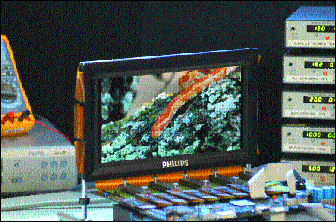
Fig. 2: This 13-in. ink-jet-printed PLED display was demonstrated by Philips at SID 2004 in May. (Courtesy of Royal Philips Electronics.)
Second, the correct volume of ink, typically a few tens of picoliters (pL), must be deposit-ed at the exact location on the substrate without overflowing and contaminating neighboring pixels of a different color. Variations in ink-drop volume may be perceived as brightness variations across the PLED display.
A typical office printer has a pixel density of up to 4800 dpi – equivalent to a local positional accuracy of about 5 μm. In principle, this accuracy is more than adequate for a full-color PLED display, which is likely to have a subpixel pitch greater than 50 μm. However, the challenge in printing displays is to have the printhead nozzles in register with the "wells" on the substrate that define the subpixels. This requires an absolute positional accuracy of a few micrometers to be maintained over the entire display surface. For a standard graphical printer, this absolute positional accuracy is neither required nor feasible.
But in the printing of PLED displays, it is not sufficient for a printer to print with high absolute positional accuracy; it must do so at high speed, printing a specified number of drops in each of a million (approximately) red, green, and blue subpixels in as short a time as possible. Any errors, such as a misplaced set of drops or an unfilled subpixel, will result in the rejection of the entire display.
Ink-Jet-Printed PLED FPDs
An ink-jet printer used in FPD production does not differ substantially from a standard graphical printer. The two main components of a PLED printer are the printhead and the motorized precision X-Y stage which moves the printhead relative to the display substrate (or vice versa). Spectra, Inc., offers an SX128 printhead which has 128 individual nozzles in a row spaced 508 μm apart (Fig. 3). It is cur-rently in use by several system integrators whoare developing PLED manufacturing lines.
Each nozzle is coupled to an ink-containing cavity with a piezoelectric driver attached to one of the chamber walls. Applying an electrical pulse to the piezo transducer produces a shock wave in the cavity that ejects a controlled volume of ink from the nozzle. Each of the 128 nozzles, which are formed as perforations in the nozzle plate, can be activated and deactivated individually, and can fire sev-eral thousand drops per second, with each drop having a volume of about 10 pL. Printing into subpixels that are closer together than the linear spacing of the nozzles is achieved by rotating the head relative to the rows of pixels.
Advances in Printhead Technology
The key development areas for ink-jet printheads are increased drop-placement and volume accuracy. Drop-placement accuracy is a function of the position of the nozzle relative to the ink "wells" on the substrate and the deviation of the drop trajectory from the normal to the nozzle plate. In order to better control the volume of LEP-ink solution deposited in each subpixel well, printhead developers are working to reduce the minimum drop volume, which effectively quantizes the volume of ink deposited. The averaging that results from printing a greater number of smaller drops into a subpixel also allows for a more-uniform volume of material to be deposited in each cell. The graphical printing industry's increasing demands for improved gray scale and variable drop control have created a large information base that is very relevant to PLED FPD printing.
Litrex Corp., followed by Spectra, Inc., has developed custom "drive per nozzle" (DPN) electronics, which allows the piezo drive waveform sent to each of the 128 nozzles to be individually tuned to allow tight control of drop volume and velocity from jet to jet. This not only increases display uniformity, but also allows smaller drops to be printed reliably; the Spectra SX128 can print drop volumes down to 5 pL using DPN-optimized control. DPN and other ink-jet-printing control implementations are enabled by the widespread commercial availability of op-amps with extremely short rise times (80 V/sec is necessary for DPN control) that were previously available only in custom ICs. The rapid development of drop-visualization systems has enabled fully automatic tuning of each nozzle through optical image analysis of ink drops under strobe illumination. This allows the velocity and volume dispensed from each nozzle to be measured and adjusted through modification of the piezo drive waveform.
Spectra's SX128 printhead is widely used in the industry in both pilot-production facilities and R&D labs. Its successor, the SX2, is in an advanced stage of development and is expectedto be launched commercially in early 2005. While the SX128 has a gold-plated electroformed nickel nozzle plate, the SX2 nozzle plate is fabricated in silicon by microelectromechanical-system (MEMS) machining.
Taking this MEMS technology a step further, the next generation of printheads – the M-class – will have a printhead module (cavities and ink channels in addition to the nozzle plate) entirely fabricated by MEMS machining and the subsequent lamination of two silicon wafers and a piezoelectric-crystal wafer. This printhead module will have 304 individually addressable nozzles with a spacing of about 280 μm, allowing printing at a native resolution of 180 dpi. It will be capable of high drop-firing frequencies; 40 kHz is being achieved routinely in prototypes, and higher-frequency operation is expected as development continues.
The use of silicon and the MEMS process for the SX2 nozzle plates in Spectra's new generations of printhead modules offers many more benefits the previous metal technology. Silicon nozzles are an improvement over electroformed nickel nozzles. They reduce the number of jet-trajectory and nozzle-placement errors, allowing far more precise and consistent deposition. Silicon nozzle plates can also be fabricated to a greater thickness, allowing far-better rigidity and dimensional stability, resulting in improved nozzle positioning and jetting accuracy. The thin electroformed nozzle plates are susceptible to permanent bowing, which brings the row of nozzles out of alignment.
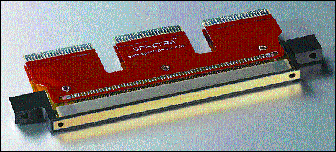
Fig. 3: The SX128 printhead from Spectra is currently used by several companies for printing PLED displays. (Courtesy of Spectra, Inc.)
The current technology has other weaknesses as well. The thin gold coating of the SX128 printhead provides chemical resistance to the solvents used to dissolve LEP materials and to the highly acidic PEDOT:PSS – the hole-transport material commonly used in PLED displays. The electroformed nozzle plate is typically 25 μm in thickness, and its soft gold coating is easily damaged by abrasion during maintenance. A thicker electroformed layer would prevent acceptable drop formation and compromise the directional accuracy of the ejected drops. If the gold layer is defective, the nozzle plate would be damaged by the acidic inks, and jetting performance would be severely compromised, requiring replacement of the entire printhead.
Spectra, Inc., is just one of the companies working to deliver next-generation printheads. Konica has developed a printhead capable of dispensing drops in volumes down to 7 pL, a figure that can be reduced to 3 pL by utilizing DPN nozzle tuning. Xaar (Cambridge, U.K.) is developing a 1000-nozzle printhead based on their proprietary "Side Shooter" technology. Each nozzle will be individually tunable and capable of variable-drop-size dispensing, based on a 3-pL sub-drop volume with eight or more levels of gray scale. The nozzle plate will have a parylene coating to protect it fromchemical corrosion, and precision construction will deliver a drop-landing accuracy of less than 5 μm at a 1-mm substrate-printhead spacing.
The printhead will be specially designed to cope with the relatively high viscosity of LEP inks and will be capable of firing up to 8000 full drops per second from each nozzle at a velocity of more than 6 m/sec. Xaar will alsointroduce the continuous recycling of ink through the channels, manifolds, and reservoirs,allowing removal of air bubbles and debris that would otherwise block nozzles or stop them from firing. The printhead is projected to be available to system integrators by Q4 '05.
Advances in Ink-Jet Printers
A PLED-display printer integrates the printhead described above with the substrate- and head-positioning systems, ink supply, and other services necessary to deposit the conjugated-polymer inks into the individual subpixel wells that form the red, green, and blue subpixels and do so quickly and consistently. Litrex Corp. (Pleasanton, California), which manufactures printers specially designed for printing PLED displays, currently produces machines capable of printing onto Gen 2 substrates (370 x 470 mm). Litrex has shippedmore than 30 of these 140P and 142P printers (Fig. 4) to display manufacturers and R&D institutions. The printers position the printhead relative to the substrate by moving it along one axis and the substrate chuck along the perpendicular axis. Litrex has also shipped20 Gen 1 machines, which are called the 80L.
The LCD industry has witnessed a rapid progression in substrate size, with a number of Gen 5, 6, and 7 plants coming on line in 2004. These vast fabrication facilities – Gen 7 glass has a size of 1.8 x 2.1 m – come with multi-billion-dollar price tags, but they ultimately reduce production costs through economies of scale. Demand for larger PLED-display screens and reduced costs will ultimately drive a similar increase in substrate sizes for PLED-display manufacture, and Litrex Corp. is developing its M-series Gen 4–7 printers to deliver this capability in 2005 (Fig. 5).
Most current ink-jet-printing machines being used to print PLED displays have a single printhead which performs multiple passes over the substrate to fill all of the subpixel wells. The complexities associated with changing inks, and the need to flush the ink system and printhead carefully when inks are changed over, generally require the use of a separate printer that is set up for each LEP-ink color and an additional printer to deposit the hole-transport material.
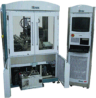
Fig. 4: This 140P ink-jet printer from Litrex is being used by Philips and OTB/Innoled in PLED-display production lines currently under development. (Courtesy of Litrex Corp.)
The key to reduced takt time – the average time it takes for a production process to produce one unit – and optimum equipment usage is the development of printers with multiple printheads that can print red, green, and blue LEP inks in as few passes of the printhead over the substrate as possible. Litrex Corp. proposes to equip its next generation of printers with 4–24 printheads, and it is developing integrated printhead and electronic control systems that will allow automated submicron alignment of multiple printheads and automatic generation of complex interleaved print patterns. The M-series printhead modules will be interchangeable, allowing off-line set up, testing, and nozzle-tuning before use. The printer downtime during printhead-module replacement will be less than 2 minutes.
The accuracy of the printer's X-Y positioning equipment plays a key role in determining the precision of ink-drop placement. Precision stage mapping is vital to ensure correct registration of the nozzles with the subpixel wells, and this is a well-developed technology for the FPD inspection-tool industry. A total positioning-system deviation of less than 5 μm is required for high-resolution display printing, and next-generation printers promise to deliver this precision. But attaining this degree of precision is difficult when large tool sizes and multi-printhead payloads are required, and it is driving a move to double overhead rails to support and position the printhead arrays.
The precision must be maintained while the printhead and substrate are accelerated and decelerated rapidly relative to each other. This rapid change in movement can also disturb the ink in the piezo pumping chambers through movement of the printhead and ink-supply tubes that connect the nozzles to the main supply reservoirs. These movements can cause nozzles to stop firing and require them to be re-primed, with the associated equipment downtime.
CDT and Litrex Corp. have developed a control system based on a local pressure-controlled ink reservoir in close proximity to the printhead nozzles, which ensures that the printer can continue to function effectively after rapid movement. This meniscus-control fluid-delivery system also provides better control over jetting at higher frequencies, and printingat 15 kHz (15,000 drops per second per nozzle) has been demonstrated using this technique.
PLEDs in Production
So far, we have looked at the currently available technologies for PLED-display production by ink-jet printing of the LEP inks and hole-transport materials as well as the developments that will allow PLED displays to be made in high volumes with high yields.
In addition to these very specific PLED tools and processes, the complete PLED-display fabrication process naturally involves substrate patterning, cleaning, and surface treatment prior to LEP printing and subsequent cathode deposition and encapsulation. These front- and back-end processes are well established in the semiconductor and LCD-panel industries, and existing toolsets are readily adapted for PLED-display production. With ink-jet-printing tools already available for printing onto Gen 2 substrates, and with parallel advances in LEP-ink formulation to enable LEP-semiconductor films to be deposited uniformly and reliably, display manufacturers are getting closer to exploiting this new production technology. But how close are they?
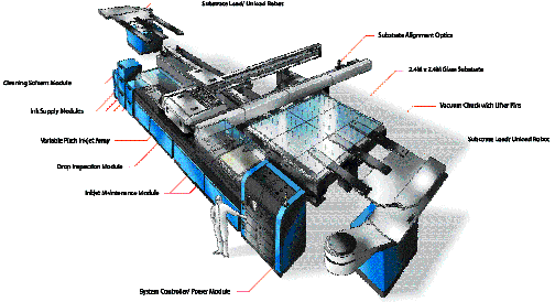
Fig. 5: This drawing illustrates the Litrex Corp. Gen 7 ink-jet-printing system. (Courtesy of Litrex Corp.)
Since mid-2003, the PolyLED team at Philips has been building a full-color-PLED-display production facility in Heerlen, The Netherlands, where the monochrome displays for the Philips Sensotec shaver are manufactured using spin-coating techniques. Philips has integrated four Litrex Corp. 140P printers equipped with SX128 printheads, which deposit the PEDOT:PSS hole-transport layer, followed by red- green-, and blue-LEP inks. Robotic handling equipment transports substrates between the four printers and to adjacent ovens that allow intermediate baking of layers when required. An integrated cathode-deposition-and-encapsulation tool completes the fabrication line.
The production line is configured to fabricate displays on a 14-in. substrate. Each substrate contains several displays, which are separated after fabrication. The fab line produces 15 completed 14-in. panels every hour, which is equivalent to a takt time of 4 minutes. The actual printing of the LEP-ink materials is not the rate-determining step in the process; handling and substrate alignment take a greater proportion of the time. Operation of the facility is completely automatic, with the system performing automated printhead maintenance and inspection to minimize engineer intervention.
During 2004, Philips worked extensively to establish the process settings and ensure that the system works reliably and produces high-quality PLED displays with a high yield. The company has developed a 1.1-in. full-color passive-matrix PLED display and plans to advance to the next stage of their roadmap and develop higher-quality larger-format active-matrix PLED displays at the Heerlen facility.
Philips is not alone in building full-color-PLED-display production facilities, although it is likely to be one of the first to ship displays to customers. OTB Engineering (Eindhoven, The Netherlands) is currently working with CDT to develop the first fully integrated and automated in-line PLED-display production facility that will be available to display companies wishing to establishtheir own PLED-display production capability.
The first system is being built for Innoled, a subsidiary of Eastgate Technology. The fab line integrates substrate patterning and pre-treatment, Litrex Corp. 140P ink-jet printers, fast cathode deposition, and thin-film encapsulation processes, and will allow significant cost reductions to be made through fast substrate throughput with minimum intervention (Fig. 6). The facility does not require a cleanroom because each tool is enclosed in a clean-air cabinet, and the facility will be capable of fabricating 30 PLED-display substrates per hour, equivalent to a 2-minute takt time.
In addition to Philips and Innoled, OSRAM Opto Semiconductors, Delta Optronics, and others are also setting up full-color-PLED-display manufacturing facilities, while several other companies are establishing advanced research activities in full-color-PLED-display production. Both Casio and Seiko-Epson have announced that they intend to begin manufacturing large-screen – greater than 40 in. – PLED-TV screens in 2007, which will require large-format printers capable of delivering a high volume of displays.
Conclusion
The unique partnership between the graphical printing industries and elements of the more-conventional display and semiconductor industries has permitted the development of an efficient and fast manufacturing process for fabricating PLED displays from solution-processable LEP semiconductors. The first commercial products from Gen 2 manufacturing facilities are expected in early 2005, and construction of larger Gen 4 and 7 production facilities are expected to begin in mid-2005. This very new manufacturing technique has rapidly reached maturity.
Disclaimer
Statements contained in this article that are not historical facts are "forward-looking statements" and their presence may be indicated by words such as "believe," "expect," "anticipate," "intend," "plan," "estimate," "seek," "will," "may," the negative thereof, and similar expressions. There can be no assurance that future developments affecting Cambridge Display Technology, Inc., and its subsidiaries will be those anticipated by management. Investors should not place undue reliance on such forward-looking statements and we undertake no obligation to update any forward-looking statements, whether as a result of new information, future events, or otherwise. The risks to our business described in our Prospectus filed with the Securities and Exchange Commission on December 17, 2004, pursuant to Rule 424(b)(4) of the Securities Act of 1933, as amended, should be considered by readers when reviewing forward-looking statements contained in this article. •
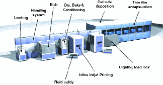
Fig. 6: This illustration shows the Innoled/OTB/CDT fully integrated in-line PLED-display fabrication system. (Courtesy OTB Engineering.)
Jonathan Halls is Strategic Technology Planner at Cambridge Display Technology, Ltd., Bldg. 2020, Cambourne Business Park, Cambridgeshire CB3 6DW, U.K.; telephone +44-(0)-1954-713600, fax +44-(0)-1954-713620, e-mail: jhalls@cdtltd.co.uk. The author thanks David Albertalli (Litrex Corp.), John Attard (Xaar), Linda Creigh (Spectra, Inc.), and Martin Fleuster and Nijs van der Vaart (Philips) for useful discussions and assistance in the preparation of this article.