Technologies for Flexible AMOLEDs
Technologies for Flexible AMOLEDs
In 2013, the world’s first mass-produced devices based on flexible AMOLED displays entered the marketplace. In this article, the technical barriers and challenges involved in creating the AMOLED panel used in LG Display’s G Flex smartphone will be described.
by Soonkwang Hong, Juhnsuk Yoo, Changhoon Jeon, Changheon Kang, Jino Lee, Joungho Ryu, Byungchul Ahn, and Sangdeog Yeo
RECENT YEARS have seen significant research investments in the development of
flexible display technology.1,2 The convergence of many critical components [substrates, barrier layers, electro-optic materials, thin-film transistors (TFTs), and manufacturing processes] is now accelerating the development of flexible displays. Many companies focused on display components are growing up around the flexible-display concept and betting on the paradigm shift to flexible in the future.
This article describes certain aspects of the development of one of the first commercially successful flexible AMOLEDs – the panel used in LG Display’s G Flex smartphone. These include flexible substrates, encapsulation techniques, the bonding process, laser-assisted release, lamination, and chamfering.
First, it is helpful to briefly consider the current and future trajectory of flexible-display development. Figure 1 shows a projected flexible-display trend from a curved and somewhat flexible device that takes advantage of the flexible panel within (available now, as with the G Flex) to future devices such as roll-to-roll and foldable displays3 that offer many potential advantages such as very thin profiles and lightweight and rugged display systems.
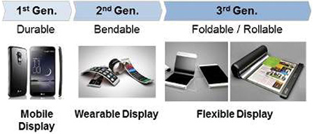
Fig. 1: Flexible displays are now enabling more mobile devices that are more resistant to shock and breakage. These displays are beginning to be used in wearable devices and will in the not-too-distant future enable foldable and rollable devices.
Flexible Substrates and ELA-TFTs
One of the first requirements for creating a flexible display is a flexible substrate, which can be either plastic or thin glass. Either must be used to replace conventional glass substrates. Figure 2 shows the basic differences between conventional glass-based AMOLED displays and plastic-based AMOLED displays in terms of their vertically stacked structures.
These plastic-based AMOLED displays are composed of a film-based backplate that is a product of an excimer-laser-annealed thin-film transistor (ELA-TFT) on a
polyimide (PI) backplane with an inorganic multi-layered buffer and an additional layer of PET underneath. This also includes a face-sealing encapsulation that can protect against moisture and oxygen while providing flexibility. The materials used for encapsulation include a barrier film and polymer layer and are shown in Fig. 4. In sum total, completely different materials, designs, processes, and equipment are required to realize the structure shown at right in Fig. 2.4
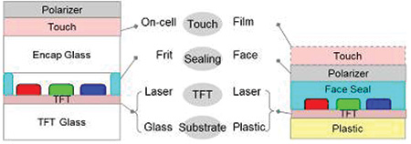
Fig. 2: The structures of a glass OLED display (left) and a plastic-based flexible OLED display (right) show not only that the latter enables a thinner panel, but that the order and composition of the stacks are very different.
Research on flexible TFT backplanes has been accompanied by studies on the effects of mechanical deformation on the TFTs.5-7 By now, the basic experimental and theoretical information required for the manufacture and use of flexible TFT backplanes has been developed. When commencing to develop our flexible AMOLED display, we reviewed with some emphasis TFTs made of low-temperature polysilicon (LTPS) ELA-TFTs for flexible displays on compliant substrates of organic polymers. The developed ELA-TFT on PI shown in Fig. 3 has been implemented with a multi-layered buffer that consists of two different inorganic layers in turn on polyimide organic material.
The realization of this structure requires a PI coating/curing process on the carrier glass, multi-layered deposition, and ELA-TFT fabrication procedures. We developed a new PI material with enough thermal durability (>500°C) for the high-temperature process for TFT fabrication. This material has a different molecular structure that gives it a bonding strength higher than is usual for PI. At the beginning stage of development, the fabricated ELA-TFT on PI had very poor reliability characteristics at a bias and temperature stress (BTS) condition of Vgs = 0 V, Vds = 20 V @ 110°C, as shown in Fig. 3. However, we finally achieved excellent reliability from ELA-TFTs on PI by optimizing the multi-layered buffer structure and process conditions as shown at right in Fig. 3.
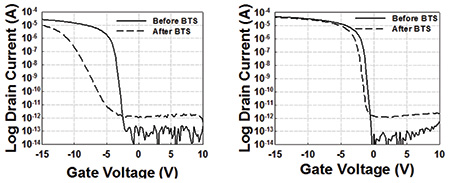
Fig. 3: Performance improvements made to ELA-TFTs on PI are apparent in this comparison of early-stage development (left) to post-optimization (right).
Encapsulation
Encapsulation is a key issue in the successful commercialization of OLEDs. Their extreme sensitivity to water-vapor-induced degradation places severe demands on the barrier performance of flexible thin-film coatings. For flexible OLED displays, frit-sealing encapsulation is not an appropriate structure because the OLEDs might be damaged by high temperatures used during the process and the frit-seal material is not intrinsically flexible.
To overcome this issue, we developed a low-temperature flexible encapsulation technology that we were able to use in a thin structure consisting of multi-layered inorganic/ organic material. We refer to this as face-sealing encapsulation, with its structure shown in Fig. 4. This structure can be used to achieve a water-vapor transmission rate (WVTR) of ~10-6 g/m2/day, which should suffice for OLED-device reliability. Furthermore, it enables high-temperature (85°C)/high-humidity (85%) storage reliability for displays. In addition, the newly developed face-sealing encapsulation structure is optically isotropic and has good light-transmission capability.
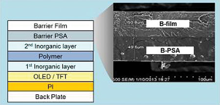
Fig. 4: The face-sealing encapsulation structure is shown at left. The image on the right is a cross-sectional view of the barrier film and barrier pressure-sensitive adhesive (PSA).
COG/FOG Bonding Process
We faced many difficulties with regard to the module bonding process. First, the chip-on-glass (COG) bonding process did not work well because the polyimide substrate exhibited high-thermal-expansion characteristics. As a result, we experienced line defects and faulty panels in the early stages of development. To avoid pressure absorption in the PI film (underneath the ELA-TFT layer), we developed a new conductive ball and higher hardness D-IC bump. We also increased the pressure on COG/ FOG (flex-on-glass) bonding as shown in the conceptual images in Fig. 5.
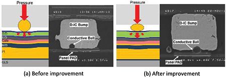
Fig. 5: Researchers improved the chip-on-glass bonding process shown in (a) before improvement by replacing the conductive ball D-IC bump, as shown in (b), after improvement.
Laser-Assisted Release and Lamination
As is well known, the process temperatures normally used during device fabrication must be much lower when working directly with plastic substrates because the heat resistance of the plastic film is much lower than for conventional glass – usually below 150°C. However, the active elements fabricated at a low temperature tend to have a lower performance than those fabricated at high temperature because high temperature is often essential to achieve a pure and defect-free material. Another difficulty of the direct fabrication process is the dimensional instability of the plastic films because these can easily expand or shrink due
to the temperature variation or moisture absorption.
In order to circumvent these difficulties presented by the plastic materials, we developed a transfer process.8,9 In this method, a high-performance and finely patterned TFT device is fabricated on a quartz or glass substrate using a conventional low-temperature poly-Si TFT (LTPS-TFT) process. Then, the TFT device is lifted off the original glass substrate and attached again to the final plastic film. Therefore, TFT performance as good as that of conventional LTPS-TFTs is expected even on the plastic film unless the TFT characteristics degrade during the transfer process. The transfer process relies particularly on a laser-irradiation technique that is favored for its high process throughput. Figure 6 shows the mechanism of a laser irradiation that lifts off ELA-TFT on PI from the original glass substrate. It uses a specific inorganic layer that plays the role of catalyst to react at the specific wavelength of the laser. When the laser irradiates the inorganic layer, hydrogen gas is released and the inorganic layer releases itself from the ELA-TFT on the PI layer. In summary, this new process allows for the temporary attachment of the PI layer to a glass carrier with a special adhesive layer that can then be deactivated after the TFT forming process using a specific frequency laser. The PI material employed, as mentioned earlier, has several unique properties that allow it to withstand the high temperatures associated with the TFT fabrication process.
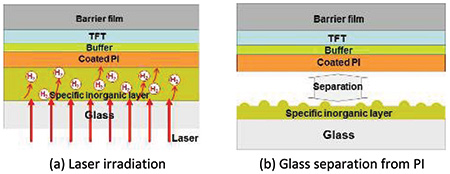
Fig. 6: (a) Laser irradiation occurs on the glass. (b) The PI/TFT layer is then separated from the glass (b).
We could achieve good TFT-on-PI characteristics by optimizing the laser-irradiation process without any performance change after laser irradiation, as shown in Fig. 7.
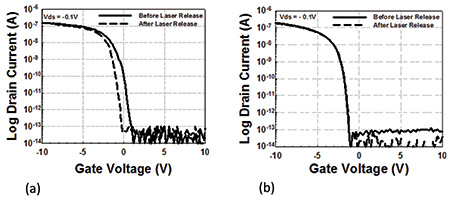
Fig. 7: (a) TFT-on-PI characteristics appear in the early stage and (b) after process optimization.
Panel Corner Chamfering
Flexible OLEDs offer some manufacturing advantages, not just challenges. One of these is the simplicity of processing the panel shape, making it possible
to reduce unnecessary areas quite easily. For example, we were able to remove the area that has no patterns in both corners of the pad in the panel through simple chamfering and laser-trimming processes, as shown in Fig. 8(a). In the early stages of development, we did have difficulty with abnormalities caused by cracks in the gate-driver-circuit clock line that is located near the chamfering line. To remove this crack “phenomenon,” we redesigned the chamfering lines by removing inorganic layers that were more brittle than others and by optimizing the chamfering process. As a result of this pad corner chamfering, we were able to realize a very narrow pad bezel design in the smart phone. Figure 8(b) shows the reduced bezel design of the G Flex phone.
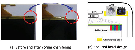
Fig. 8: In (a), the result of chamfering one of the panel corners is displayed. The schematic in (b) shows how it was possible to reduce the bezel size after the chamfering.
Physical and Electrical Reliability Issues
In order to achieve the desired reliability, a new panel design rule was also required. This new approach takes into account the face-sealing encapsulation structure and materials, especially, in the non-emissive area or the bezel. As shown earlier in Fig. 4, the face-sealing encapsulation for the panel consists of three layers: inorganic/organic/inorganic. The organic material is a specific polymer that plays a role in smoothing over height differences due to particle contamination or uneven surface conditions.
It was not easy to prevent particle-cover-layer (PCL) overflow failure from the screen coating process at the end of the bezel region. In this case, the second passivation layer could not cover the entire polymer layer; as a result, water permeation occurred at the area as shown in Fig. 9(a). We added a dam to this area in order to avoid the type of moisture penetration problem shown in Fig. 9(b).
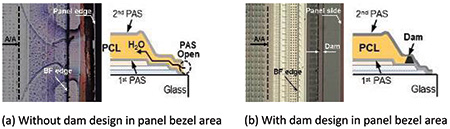
Fig. 9: A dam was added (b) to the bezel area of the panel in order to prevent PCL overflow (a).
In the early stages of development, we also had difficulty with display abnormalities that stemmed from the integrated gate driver circuit malfunctioning after hundreds of hours of operation at high temperature and high humidity. The root cause was low thermal conductivity of the multi-layered buffer and polyimide that accelerated TFT degradation due to channel self-heating. To achieve electrical reliability, we optimized the circuit design by considering the characteristics of ELA-TFT on PI under thermal and bias-stress conditions. Figure 10(b) shows improved gate driver output waveform under accelerated driving condition.
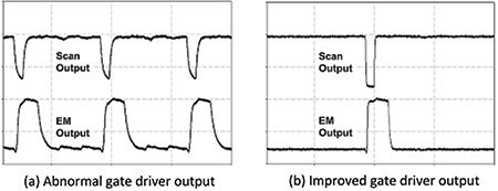
Fig. 10: (a) The gate driver demonstrated abnormalities under conditions of high temperature and high humidity. At right, (b), it shows improved output as a result of optimized circuit design.
Successes and Further Challenges for Flexible OLED Displays
Figure 11 shows a flexible display panel and the commercialized smartphone (the G Flex) that was launched on a 5.98-in. flexible OLED manufactured by LG Display. Compared to other flat-panel displays, this panel has very thin, light, and bendable characteristics. Even the smartphone itself has some flexibility.
The processes and materials we developed – ELA-TFT on PI and face-sealing encapsulation with a new panel design, the optimized COG/FOG bonding process, and the laser-induced carrier glass release and back-plate lamination process – enable the efficient mass production of flexible OLED panels that are reliable enough to be used in commercial products. Having been successful in overcoming so many technical barriers and challenges to realize this product, we are confident in the overall future of flexible OLED displays.
The OLED panel shown in Fig. 11 has a bending radius capability of about 15 mm, though when integrated in a smartphone the construction of the device limits that bend-ability to a certain degree.
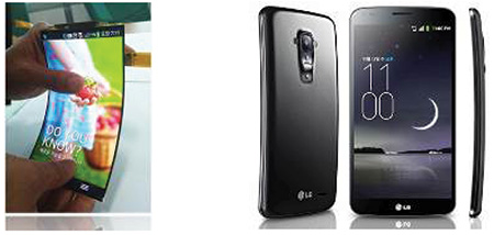
Fig. 11: LG’s 5.98-in. flexible OLED panel (left) appears in its G Flex smartphone (right).
With regard to further challenges in flexible-OLED-display design, we are currently focusing on several technologies. First, we need to achieve more flexibility and robustness. For the backplane, new materials for the TFT layer and pattern design optimization are necessary. Also, new materials and face-sealing structures are needed for increased flexibility of encapsulation. We are also considering touch on barrier-film structures and new touch-sensor materials. Film thickness reduction of the polarizer, barrier film, and backplate is also a key challenge. However, we believe that the product designs that can be achieved with flexible OLED displays, such as the foldable and bendable displays discussed earlier in this article, will not only enable emerging smart devices, but trigger an entirely new field of innovations – products and technologies not yet imagined.
References
1B. Kim, Y. H. Jang, S. Y. Yoon, M. D. Chun, H. N. Cho, N. W. Cho, C. Y. Sohn, S. H. Jo, C. Choi, C. D. Kim, and I. J.Chung, Proc. IDW, 1073 (2005).
2S. H.Paek, Y. I.Park, C. H.Park, Y.S. Lim, S. I.Shin, C. D.Kim, and Y. K.Hwang, SID International Digest of Technical Papers, 1047 (2010).
3http://www.yankodesign.com, http://designbuzz.com, http://www.coroflot.com
4G. P. Crawford, Flexible Displays (Wiley, 2005).
5P. H. I. Hsu, M. Huang, S. Wagner, Z. Suo, and J. C.Sturm, Materials Research Society Symposium Proceedings 621, Q8.6.1-Q8.6.6 (2000).
6P. H. I. Hsu, R. Bhattacharya, H, Gleskova, M. Huang, Z. Xi, Z. Suo, S. Wagner, and J. C. Sturm, Applied Physics Letters 81, 1723–1725 (2002a).
7P. H. I. Hsu, H. Gleskova, R. Bhattacharya, Z. Xi, Z. Suo, S. Wagner, and J. C. Sturm, Materials Research Society Symposium Proceedings, paper G1.8 (2002b).
8T. Shimoda and S. Inoue, “Surface free technology by laser annealing (SUFTLA),” IEDM Technical Digest, 289 (1999).
9S. Utsunomiya et al., “Low-temperature poly-Si TFTs on plastic substrates using surface free technology by laser ablation/annealing (SUFTLA),” SID International Symposium Digest of Technical Papers 31, 91 (2000).
Soon-Kwang Hong is currently a Research Fellow at LG Display Co., Ltd., as Head of the PO Product Development Department. His research interests include electrical circuit driving, compensation schemes and structures, and materials and processes related to glass-based and flexible AMOLED displays. He can be reached at skhong@lgdisplay.com.