Part I: A Brief History of Key Areas in Display Technology
In Part I of our 50-Year Anniversary Special Coverage, display-industry experts outline the history of displays through parallel technology developments.
FOR this special 50th anniversary article, Information Display asked six display-industry experts to share their knowledge and perspective of specific areas of display technology: cathode-ray tubes (CRTs), projection, early roots of liquid-crystal displays (LCDs), active-matrix LCDs (AMLCDs), plasma display panels (PDPs), and organic lightemitting- diodes (OLEDs). Some of the technologies CRTs, for example were once dominant but have since been eclipsed by others. However, something that becomes clear from reading these entries is that no one technology succeeds completely independently of another. For example, without knowledge gained from designing CRTs, developers would have had a much harder time creating, or even imagining, todays LCDs. Backplane advances that enabled better LCDs have now helped realize larger OLED displays as well. Todays technology will, in turn, bolster the displays of the future displays we can only guess at today. We hope you enjoy the following stories, told from the standpoint of industry veterans who experienced these technology shifts firsthand.
CRT Retrospective
Not so long ago, to speak of a display was to speak of a CRT. The industry owes a tremendous debt to the developers and manufacturers of CRTs.
by Chris Curtin
Reviewing the cathode-ray tube (CRT) as part of SID's 50th anniversary takes one on a bittersweet journey. Initially, and for a large segment of the past 50 years, the CRT was the major topic at SID meetings and the only display device in TV factories around the world. By 2012, the CRT has become a footnote in the realm of display device development.
The evolution of the color CRT for TV receivers ranks as the most significant impact of this technology in the last 50 years. By the early 1960s, the three-beam shadow-mask design was the foundation for continual increases in screen size, color purity, resolution, luminance, and cost reduction to satisfy consumer requirements. Most significant of the system-engineering improvements was the increase in luminance over a 20-year period as shown in Fig. 1.
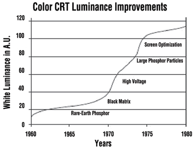
Fig. 1: Color CRT luminance increased dramatically over the period between 1960 and 1980. Source: SID 50-year history committee timeline (CRTs), www.sid.org.
While not of the same magnitude improvement, the scaling up of the color-CRT screen size to 36 in. and beyond in the 1990s represents a major advance in glass faceplate and bulb design as well as electron gun, magnetic deflection yoke, and shadow-mask/grid design.
The developments for color-TV viewing provided the foundation for higher-resolution CRTs required for computer graphics and computer-aided design. In the early 1980s, the price of solid-state memory (RAM) decreased to the point where computer-based workstations using color CRTs became common. As costs were reduced further, the personal computer evolved from monochrome to color CRTs, initially at 13 in. on the diagonal and eventually to 19–25 in. on the diagonal. The CRT's color purity and ability to match the output of color printers set standards for flat panels as they began to replace CRTs in workstations and PCs in the 1990s.
Major CRT developments were also made for oscilloscopes, medical imaging, radar, avionic cockpits, and large-screen projection systems. As the electronics industry boomed during the 1960s, electrostatically deflected CRTs for oscilloscopes helped lead the way with ever faster response times, culminating with the addition of a micro-channel-plate multiplier to allow photography of single-shot signals moving at the speed of light. Before the era of solid-state memory, storage CRTs served to capture and display transient events. An important spinoff using the phosphor-storage technology was the high-resolution monochrome graphic computer terminal in 11-, 19-, or 25-in. models, which dominated the field until the price of solid-state memory dropped to a competitive point in the 1980s. Hardcopies of the graphic display were obtained via a fiber-optic line-scanned CRT exposing dry silver paper.
High-resolution electron guns developed for computer graphics enabled specialized monochrome CRTs for medical-imaging applications such as digital radiography, ultrasound, and nuclear medicine. The avionic "glass cockpit" required extremely high brightness to overcome the sunlight that often shone on the display screen. High-current electron guns and high voltage on the phosphor screen along with a rugged shadow-mask design combined to satisfy this need.
Projection CRTs had dual roles, one for large-screen TV and another for flight simulators and control rooms. While the sales volumes were modest compared to the shadow-mask color CRT, this was the major route to large-screen displays in the last century. Typically using three small monochrome CRTs (red, green, and blue), very high intensity was needed to achieve adequate luminance at the final screen. Light valves that separate the addressing function (the "valve") from the light-generation function (light bulb or LED or laser) eventually replaced CRTs as the "projection engine" by offering more performance at a comparable price.
(More details, including some of the companies involved, appear on the "CRT timeline," which can be found, along with timelines for plasma, projection, LCD, AMLCD, and OLED, at www.sid.org. These advances required literally thousands of scientists, engineers, and technicians around the world, some of whom were formally recognized by the SID and are included in the timeline.)
Major developments in literally hundreds of electron-beam devices or technologies were completed during the last 50 years. In the end, the bulk and size limitations dictated by the mechanical requirement to support the atmospheric pressure limited the traditional CRT's application and markets. Long viewed as the "ultimate goal," flat and thin CRTs saw significant development in the 1990s using a screen-sized matrix array of cold-cathode field emitters. However, the improving performance and decreasing costs of LCDs ended the CRT's competitive threat at the beginning of this century.
Chris Curtin has worked on CRT design and manufacturing since 1963. Beginning in 1989, he helped develop the field-emission display until retiring in 2001. He can be reached at ccurtin@rockisland.com.
A Look Back at Projection
Pico-projectors and micro-projectors will outpace, but not replace, mainstream projectors within the next few years.
by Matt Brennesholtz
Projection Before SID
From 1902, until before the Society for Information Display was founded in 1962, electronic-display technology was dominated by the cathode-ray tube (CRT). The first CRT television sets, both direct-view and projection, were available before World War II. The war largely put an end to consumer use of TVs but also led to rapid changes and improvements in CRT technology. For example, radar systems developed during the war played a major part in the Battle of Britain and required CRT displays for their operation.
Following the war, there was a resurgence in television and projection technology for entertainment use. Perhaps the ultimate expression of the large-screen CRT projector was an RCA tri-color receiver-projector developed by Dr. David Epstein, which provided theater-sized screen images. This behemoth was built in 1951 to demonstrate NTSC color-TV signals in a theatrical environment.
The CRT was not the only available display technology suited for projection, however. The Scophony projector from the 1930s was a surprisingly modern, mechanically scanned projection system based on rotating drum mirrors, an arc lamp, and an acousto-optic modulator. Scophony systems were used in a few movie theaters for live events, but plans to build a home version of this projector died when the war started.
Oil-film light-valve projection had its origin in the prototype system built at the Swiss Federal Institute of Technology in Zurich and was demonstrated on New Year's Eve in 1943. This technology eventually grew into the Eidophor projection system, which became a commercial product in 1958. A competitive oil-film system from General Electric, the Talaria, was also introduced in 1958. (Augustine Albanese from GE presented a paper on this system titled "The Light-Valve Projection System" at the initial SID technical meeting in 1963.) These systems were capable of producing much higher light outputs than CRT projectors and dominated the high end of the projector market until they were replaced by LCD-based projectors in the early 1990s. The Talaria finally went out of production in 1994 and the Eidophor in 1997.
The Early SID Years: CRTs and Light Valves (1962–1992)
SID was founded in 1962 and held its first two technical meetings in March and October 1963 in California and New York, respectively. Projection was a part of the Society right from the start. In the March meeting, 4 of the 13 technical papers presented were directly related to projection, including one given by the current SID historian, Pete Baron. In the October meeting, 3 of the 15 presented papers were on projection topics, including one on laser projection. Overall, for these first two SID meetings, 25% of the technical papers were projection related.
Early in these years, interest in large-screen CRT projection was low because of the superior performance of oil-film light valves. During this period, the CRT projector was mostly limited to professional applications where the screens were not large enough to justify the use of a light-valve projector.
The lull in consumer CRT projectors ended in 1972 with the introduction of the Advent VideoBeam projector with Schmidt optics, developed by Henry Kloss from a design by Art Tucker. Liquid-crystal light valves (LCLVs), also known as light amplifiers, began to compete with oil-film light valves for the large-screen market in 1972, with the development of a LCLV projector by Hughes for the U.S. Navy. Early units had slow response times, but by 1977 Hughes had developed a three-light-valve system suitable for showing color television images. This LCLV technology eventually developed into what is known as liquid crystal on silicon (LCoS) today.
Toward the end of this period, a number of companies, including Sharp, Barco, and Seiko Epson, introduced projectors based on liquid-crystal devices. These LCD projectors had marginal performance in terms of resolution, light output, and contrast, even compared to the standards of the time. But they were more portable than either the CRT or light-valve projectors of the time and they presaged the coming revolution in projection technology.
Microdisplay Projection (1992–2012)
Two events, one in 1992 and the other in 1993, doomed CRT and light-valve projection. First, in 1992, Barco introduced the BarcoData 5000 projector, popularly known as the "Light Cannon." This was the first LCD projector that had performance comparable to light-valve projectors. It was large and expensive to buy and operate but not as large nor as expensive as oil-film or LCLV systems with comparable performance. Oil-film systems have vanished from the projection landscape, but LCLV technology survives as LCoS. The BarcoData projector could hardly be called a microdisplay projector, however, with its 5.8-in. panels.
The étendue issue, or the relative size of the light source and the projection microdisplay, was essentially solved by Philips in 1993 with the introduction of the UHP lamp. This lamp had a mercury fill and produced light from a very small volume of space, with an arc length not much more than 1 mm long. The UHP also had a very high efficacy and long life, compared to other short arc lamps in use such as xenon. This small arc size enabled an explosion of microdisplay-based projectors that used LCD, DMD, or LCoS technology.
Another important 1993 milestone was the demonstration of a 768 x 576 color-sequential digital micromirror device (DMD) by Texas Instruments. The DMD was so popular that the 1994 SID symposium devoted an entire session to it. The first commercial DMD-based color-sequential projector was introduced by Barco in 1996.
Texas Instruments and Hughes/JVC began the digital-cinema revolution in 1999 with the first digital-cinema projectors, such as the unit shown in Fig. 2.
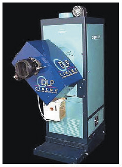
Fig. 2: This DLP projector used in 1999 digital-cinema tests was mounted on a Christie xenon-lamp lighthouse and was originally designed for a film projector.
Projection into the Future (2012 to ?)
The display industry has grown, to put it mildly, and the most recent SID Symposium in Boston drew 426 technical papers, about 24 of which directly related to projection technology for a total of 6% of the papers, down from 25% during the 1963 high point. This does not necessarily mean that projection technology is on the wane; it is just an indication of the rising importance of direct-view display technologies. For example, when the Society was founded in 1962, telephones did not have displays. Now, roughly 1.7 billion cell-phone handsets will be sold in 2012 and every one of those handsets has at least one display.
Projection technology has always been about large-screen images, which, in 1962, meant images larger than about 21 in. Today, mainstream electronic projection technology is rarely used for images smaller than about 60 in. Direct-view plasma or LCDs up to about 150 in. on the diagonal are available, if not affordable. Still larger direct-view displays in sizes limited only by your budget are available using LED arrays. These displays can easily show an instant replay of a football goal to 100,000 screaming fans in a stadium.
When given a choice between projection and direct view, most end users select a direct-view display unless the price differential is too high or there is some other reason why a direct-view display is unsuitable. This has given rise to a market for small pico-projectors and micro-projectors suited for making images in the 20–60-in. range.
Why would anyone want a 20-in. projected image when a 20-in. computer monitor can be purchased from a respected brand for $100? The answer here is convenience – a 20-in. monitor and its power supply cannot fit into your pocket. A pico-projector that generates a 20-in. image will not only fit into your pocket but within a year or so it will fit inside a cell phone. If the 4-in. display in a handset or the 10-in. display in a tablet just is not big enough, a pico-projector will provide a larger image, certainly 20 in. and maybe larger, depending on the ambient light.
By unit volume, forecasts indicate pico-projectors and micro-projectors will outrun mainstream projectors within the next few years, but mainstream projectors are not going away. The fastest growing market for mainstream projectors in the 2000–5000-lm range is education, although other professional AV markets remain strong as well. An example of a modern professional AV projector is shown in Fig. 3.
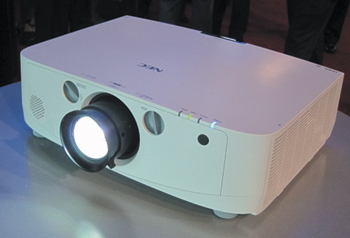
Fig 3: This NEC NP-PA500U 5000-lm installation projector is for larger conference rooms and auditoriums. This projector is based on three 0.76-in. LCD microdisplays, each with a resolution of 1920 x 1200 pixels. At $5899, this projector costs about 10% of what a 1992 1000-lm, lower-resolution Talaria oil-film projector cost.
Electronic projection technology has evolved since it was first demonstrated in 1902 with a 12.5-line scanned image and since SID was founded in 1962. Near-term and "distant future" goals for projection displays were given by Anthony Rugari in his 1963 paper titled "Laser Display Techniques," as shown in Fig. 4. Clearly, we are already well beyond the "Distant Future," at least in terms of projection displays.
| |
Near Future |
Distant Future |
| Resolution |
one million elements |
four million elements |
| Highlight brightness |
50 fL |
100 fL |
| Contrast ratio |
10:1 in dark |
100:1 in dark |
| Screen size |
10 ft x 10 ft |
20 ft x 20 ft |
| Color |
one color with five distinct shades of the color |
7 colors: white, red, green, blue, magenta, cyan, yellow |
| Update time |
30 frames/sec |
30 frames/sec |
Fig. 4: Shown are near-future and distant-future goals for projection displays from about the time that SID was founded. Source: A. D. Rugari, Laser Displays Techniques, Society for Information Display (October, 1963).
The need for large, bright, high-resolution, affordable images has not gone away even though the market definitions of "large," "bright," "high-resolution," and "affordable" have changed since SID was founded. Therefore, projection displays have not gone away nor are they expected to go away in the foreseeable future.
Further Reading
Large parts of this article are based on the paper the author published in the Journal of the SID in October, 2007. This article wasreprinted in two parts in Information Display in the May and September 2008 issues. The Projection Time Line, originally developed in 2010 and available at www.sid.org, was updated in 2012 and re-issued in honor of SID's 50th anniversary.
Matt Brennesholtz is an analyst at Insight Media. He can be reached at matthew@insightmedia.info.
Evolution of the LCD in the UK
The contribution of UK researchers to the development of LCDs have been substantial and fundamental.
by Peter Raynes
The UK has an enviable reputation for its contributions to the development of liquid-crystal displays (LCDs) and the pre-eminent position they now hold as the display of choice for most office and consumer-electronics equipment. These contributions have been remarkably interdisciplinary, ranging through mathematics, physics, chemistry, and engineering.
The first major contribution to emanate from the UK was the first-ever patent for an LCD, written by B. Levin and N. Levin, and granted in 1936 to the Marconi company. The next major contributions, from academia, were made after some 20 years had elapsed and laid out the continuum theory of nematic liquid crystals. The static theory was developed by Sir Charles Frank in 1958, and in 1968 Frank Leslie transformed it into the dynamic theory. The continuum theory is the bedrock of the vast amount of numerical modeling of LCDs employed by the industry in the development and optimization of the vast array of LCD modes currently available.
There then followed approximately two decades of discoveries and inventions from within a consortium of academia, industry, and government laboratories, which attacked the many challenges of the early simple LCD technology and laid the foundations for the multibillion-dollar industry of today. This consortium was formed and guided by three wise and determined individuals: Cyril Hilsum at the Royal Signals and Radar Establishment, George Gray at Hull University, and Ben Sturgeon at BDH Chemicals.
The early liquid-crystal materials were unstable, colored, and quite unsuitable for use in displays. In 1972, this changed dramatically when cyanobiphenyls were invented at Hull University. These stable, colorless materials had excellent device properties and, once they had been formulated into wide-temperature-range mixtures, they quickly became the material of choice of the LCD industry. Supplemented by the later addition of mixtures tailored for multiplexed displays, the cyanobiphenyls held dominance in the industry for more than a decade and resulted in two Queen's Awards for Industry to the groups involved.
Two improvements of the basic twisted-nematic (TN) device quickly followed from the consortium. The detailed optics of the device was understood and an equation derived that allowed the design of LC materials for thinner and superior TN devices. Secondly, early TN devices showed non-uniform contrast quite unacceptable to the consumer. The origins were traced to degeneracies in the liquid-crystal alignment and techniques found to remove them. These techniques and the design of materials for the superior thin devices became industry standards still in use today.
Toward the end of the consortium, two breakthroughs occurred that were key to the transformation of LCDs into the high-information-content displays so familiar today in mobile phones, computers, and televisions. It had become increasingly obvious to all concerned that the electrode sharing technique known as multiplexing did not work at all well for liquid crystals, and the prospects for using LCDs in phones, computers, and televisions looked rather dim. The reason for this difficulty lay in the response of liquid crystals to electric fields; they respond to the root mean square of an applied field, making multiplexing and high-information-content displays virtually impossible. Within a short space of time, two quite different ways forward were opened up and transformed the industry. The increase of the twist angle of the TN device produced a device with such a steep response that multiplexing became possible; this device attracted the name supertwist, or STN device. Secondly, the long-held view that electrical driving elements should be used to individually switch each pixel suddenly became a practical reality with the development of amorphous-silicon thin-film transistors (a-Si TFTs) at Dundee University. Although Dundee lay outside the consortium, the key development arose as input from within the consortium. At Dundee, Walter Spear and Peter LeComber had been developing a-Si material technology, but thought the application applied to solar cells. The consortium thought differently, and encouraged and financed the fabrication and testing of the world's first a-Si TFT-LCD array. Both technologies are still in use by the LCD industry; but the early dominance of the STN, which was easy to fabricate with existing technology and launched many new applications, was soon replaced in many of these by the superior, but much more difficult to manufacture, a-Si TFT technology.
Numerous developments subsequent to the consortium emanated from the UK. Chemists at Hull synthesised new LC materials, which became used in the ever-diversifying range of LCDs. The use of the difluorophenyl ring in difluoroterphenyls and other materials has become widespread in LC mixtures designed for one of the LCD modes in widespread use in televisions, the vertically aligned nematic, or VAN display, and its derivatives. Optical compensation films are universal additions to improve the optical performance of LCDs. Many optical compensation films incorporate materials that are derivatives of triphenylene discotic compounds with a negative optical birefringence. Ferroelectric LCDs, once seen as the great hope for high-information-content displays before the inevitable march of a-Si TFTs, owe much to UK development. The chemists synthesised new FLC materials and physicists developed an understanding of the devices and found ways of overcoming some key fabrication and driving issues. Recently, there has been a resurgence in niche applications of FLCDs, such as projectors, SLMs, and cameras.
Bistable displays, which maintain an image long after the removal of driving signals, had for some time been a goal of the LCD industry, and many options had been considered and rejected. Device physicists at RSRE, which by now had become DERA, and later QinetiQ, came up with a novel device configuration and switching mechanism known as the Zenithal Bistable Display, or ZBD. This device is truly bistable with a very attractive appearance; it is being tested for supermarket shelf labels and has yet to reach its full potential. (See the article "Approaching the "Zenith": Bistable LCDs in a Retail Environment" in the March 2009 issue of Information Display.)
Over the years, the UK output of key contributions has been recognized by numerous SID awards. The lists of winners of the Karl Ferdinand Braun and Jan Rajchman Prizes, the Special Recognition Awards and SID Fellows, and Senior Members contain many UK names, demonstrating the international recognition of the many contributions made by UK researchers to LCD technology.
Peter Raynes is a Leverhulme Emeritus Research Fellow and an Honorary Visting Professor in the Department of Chemistry, University of York. He was previously at Oxford University, Sharp Laboratories of Europe and RSRE Malvern. He was awarded SID's Jan Rajchman Prize, a Fellow-ship and a Special Recognition Award for his research on liquid-crystal materials and displays. He can be reached at peter.raynes@york.ac.uk.
Active Matrix and the Evolution of LCDs
Active-matrix technology has played a crucial role in the commercial success of LCDs.
by Lawrence E. Tannas, Jr.
At the time of the founding of SID in 1962, the display industry was about to embark on a paradigm shift. In the beginning, electronic displays such as galvanometers and CRTs were analog indicating transducers. Today, electronic displays such as plasma panels and LCDs are digital-matrix arrays of randomly addressable pixels. The year 1992 can be considered the mid-point in the process by which AMLCDs replaced CRTs as the primary electronic information display. One key event occurred at the Japan Electronics Show in 1988. Both Sharp and DTI (a consortium formed by 50% Toshiba and 50% IBM) predicted the future with their display of 14-in. AMLCDs in full color, using amorphous-silicon as the active-matrix element. Japan had become the leader in electronic displays – a transition that was obvious at SID's 25th anniversary.
Sharp's speculative venture to build the first Gen 1 AMLCD factory in 1992 was electrifying. Most industrial leaders conceded that the technology was feasible but believed the cost would be prohibitive. It was unimaginable then that one could manufacture a half-million transistors on a single substrate with very high yield. These days, Sharp is operating a Gen 10 AMLCD factory with 3 million transistors per substrate.
Matrix Addressing
The history of the evolution of LCDs as flat-panel displays was paced by the evolution of active-matrix addressing using active elements at each pixel. This combined embodiment is referred to as the ubiquitous active-matrix liquid-crystal display (AMLCD). A TV image is easily implemented on a CRT because the image is created by scanning an electron beam left to right, top to bottom, using passive analog techniques. At any one point on the screen, the image is only active for a very small fraction of the frame time, but the image appears continuous to the user because of the combination of the very bright persistence of the phosphor and the refresh rate. This method of drawing an image on an electronic display is called scan-line addressing.
The first generation of LCD panels also used this technique, often called passive-matrix addressing, where the pixels were individually updated one at a time from the upper left of the frame, line by line from top to bottom. However, unlike CRTs, this approach resulted in displays with relatively low contrast and poor video performance, although they were an outstanding achievement at the time. It wasn't until 1986 that the first AMLCD was mass-produced for a small handheld video player when a-Si transistor technology and LCD technology were merged into the modern AMLCD. Active-matrix addressing allows the video data for each pixel to be stored at that pixel location. The pixel remains at its intended value for the entire frame time, greatly improving contrast and opening the door for fast response times and full-motion video rendering.
In 1988, Tsamu Washizuka received the IEEE Ibuka Award for Sharp's 14-in. full-color full-motion display. Photo courtesy Sharp.
Evolution of LCDs
Some of the key milestones on the timeline of LCD technology evolution can be studied further by researching these topics:
• Discovery of the Williams Domain in LC material, Sarnoff Labs, 1962
• Invention of the twisted-nematic mode of LCDs, 1971
• Evolution of mathematical modeling of LCDs
• Synthesis of cyanobiphenyl LC material in 1972
• Continuing improvement in LCD design, in-plane twist, compensating films, TFT structure, 3-D, LED backlights, backlight addressing, high-frequency refresh, over-voltage addressing, etc.
Observations on AMLCDs
• It took 30 years for a-Si AMLCDs to evolve and another 20 years for their performance details and production technology to be perfected; Sharp in 1990 demonstrated "TV on the Wall," and in 1992 proved the manufacturability of a-Si LCDs.
• AMLCDs required international collaboration among companies, laboratories, and people; the center of activity moved from the U.S. and Europe to Japan and, now, Korea, led by Samsung and LG.
• Competition has continued, with plasma panels initially being used for the very large display market and passive LCDs and AMOLEDs for the smaller-display market. Today, LCDs are displacing plasma panels even in sizes up to 90 in., and AMOLED displays are being positioned to challenge LCDs in 55-in. TV; AMOLED displays and LCDs are competing in the recently created market for very-high-quality small- and medium-sized displays for smartphones and tablets.
The Future
Clearly, AMLCDs are the leading technology today just as CRTs were until 1992. Active-matrix OLEDs (AMOLEDs) have now been publicly demonstrated to show superb performance at potentially a lower cost in 55-in. sizes by Samsung and LG. It's similar to the 1990s all over again. Highly skilled display engineers are split on how the future may evolve. Again, the answer rests in the techniques used in matrix addressing, and the stigma of poor life performance in OLED materials has not been eliminated. In any event, the future is bright. AMLCDs will be getting better and AMOLED displays show promise as the next generation of displays.
Lawrence E. Tannas, Jr., is President of Tannas Electronics, a Fellow and Past-President of SID, and Chairman of the SID 50th Anniversary Celebration Committee. He can be reached at l.tannas@tannas.com.
The First Plasma-Display Product
Today, flat-panel displays dominate our industry, but in 1962, the year SID was founded, very few flat-panel products existed, even though the desire for practical flat panels for hang-on-the-wall TV was strong. This is the brief story of the development of the first plasma-display product, which is the ancestor of all of the flat-panel TVs we have today.
by Larry Weber
As with any invention, it all started with a need. In this case it was the need for a high-quality display for computer-based education. The University of Illinois started a project in 1960 called PLATO (Programmed Logic for Automatic Teaching Operations) to conduct research on the use of computers for education.1 It was a pioneering project on a topic that now seems obvious. It was clear to the leaders of the PLATO project that a graphics display was a necessary component for computer education.
However, in those days even a simple alpha-numeric computer terminal was a real luxury. The common method for man–machine interface was the teletype and the punched tape.
In 1964, the "advanced technology" PLATO 3 system used CRT-based graphics display terminals with external scan converter memory tubes originally designed for FAA radar as the bitmap storage. This was one of the few viable bitmap storage technologies of that era. Of course the semiconductor memory that we now use in our PCs and laptops had not been developed yet.
The plasma display panel was invented by Prof. Donald L. Bitzer, Prof. H. Gene Slottow, and their graduate student Robert H. Wilson in 1964 to meet the need for a full-graphics display for the PLATO system.2 One of the key goals of this new graphics display invention was to have inherent memory so that the bulky and expensive scan-converter tube memory could be eliminated. This first single-pixel device used neon gas to generate the familiar orange glow. Fortunately, the vacuum system used to evacuate the panel had a leak that added a small amount of air to the neon. This gave the discharge a hysteresis characteristic that inventers quickly recognized would be useful to achieve their goal of inherent memory. Pure neon gas without the leak did not have this hysteresis. The practical solution for panels that did not leak was to add a fraction of a percent of nitrogen to the neon to achieve inherent memory. Today's plasma TVs use inherent memory to hold the image during the frame time. This eliminates the need for an active-matrix transistor for each pixel.
Figure 5 shows the first plasma panel with more than one pixel. This result was first published in 1966.3 It was a major achievement since it was also the panel that demonstrated the first matrix addressability.4 The inventors named this invention the "plasma display panel."
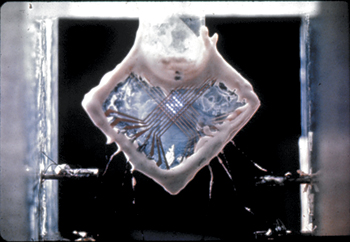
Fig. 5: This early 4 x 4-pixel panel was presented in the first publication on the plasma-display panel by the University of Illinois in 1966.3 This panel was the first to have more than one pixel. It was also the first to achieve matrix addressability.4 The outer dimensions of the panel are 1 in. square. Photo courtesy Donald Blitzer.
As a young graduate student, I can remember making this kind of device with the very fragile 150-μm thin sheets of glass and the vacuum epoxy that can be seen glopped around the perimeter. When I would evacuate the air from the panel, the external atmospheric pressure would usually break the thin glass. Fortunately, this could usually be repaired by applying more epoxy. Even then my devices would die after 2.5 hours due to gas contamination from leaks and I would have to periodically put in fresh gas. This was certainly not a manufacturable device.
First Product
In the next few years, a number of industrial companies continued to work toward practical products. These included Owens-Illinois, IBM, Control Data, and Fujitsu. Owens-Illinois won the race in 1971 by delivering the first practical product, which is shown in Fig. 6. The first customer was appropriately the University of Illinois PLATO project. This product was a 512 x 512 pixel-array full-graphic display having a square aspect ratio and a diagonal of 12 in.5 It used the much more robust panel structure Owens-Illinois had pioneered in 1968. The glass plates were now a rugged 6 mm thick and the all-inert-gas mixture was hermetically sealed in with solder glass instead of epoxy. I still have some of these panels and the gas has not become contaminated even after 40 years.
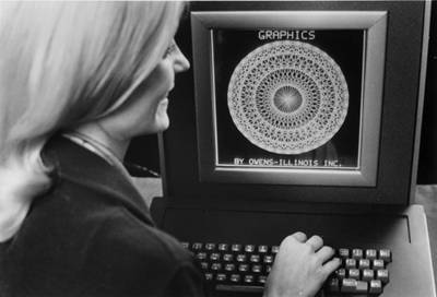
Fig. 6: Owens-Illinois delivered the first plasma-display-panel product to the University of Illinois in 1971. It was a 12-in.-diagonal 512 x 512-pixel full-graphic display with inherent memory. Photo courtesy Owens-Illinois.
The period from the initial invention of the plasma panel in 1964 until the first product delivery in 1971 was remarkably short. (This concept is reinforced by a quick comparison of Figs. 5 and 6.) By 1975, Owens-Illinois had delivered 1000 of these panels to the University for its PLATO 4 system, which could simultaneously control all 1000 graphics terminals with one computer mainframe.6
Further Developments
Over the next 15 years, other companies such as IBM, Fujitsu, NEC, Control Data, Electro Plasma, Photonics, Plasmaco, and AT&T developed more advanced monochrome products that worked on the same principles.7 The PDP color age started when Fujitsu introduced its 21-in.-diagonal full-color plasma-panel product in 1992 and its 42-in.-diagonal color TV in 1996. Because of strong competition from the LCDs, plasma manufacturers developed the winning strategy of making large-diagonal (42-in. and larger) TV displays. This was not initially possible with AMLCD products. The great success of these plasma products demonstrated that the biggest market for flat-panel displays was for large-screen TVs. The success of the plasma panels in this giant market soon attracted the LCD manufacturers,who followed with their own large-screen TVs. So, not only are the technologies found in the first plasma-display product used in every plasma TV sold today, but this first product also had a major impact on today's LCD TVs.
References
1D. Alpert and D. L. Bitzer, "Advances in Computer-based Education," Science 167, 1582-1590 (March, 1970).
2D. L. Bitzer, "Inventing the ac Plasma Panel," Information Display 15, 22-27, (February, 1999).
3D. L. Bitzer and H. G. Slottow, "The Plasma Display Panel: A Digitally Addressable Display with Inherent Memory," Presented at the 1966 Fall Joint Computer Conference, Washington, D.C., AFIPS Conf. Proc. 29, 541-547 (1966).
4B. M. Arora, D. L Bitzer, H. G. Slottow, and R. H. Wilson, "The Plasma Display Panel: A New Device for Information Display and Storage," SID Symposium Digest (May, 1967).
5H. J. Hoehn and R. A. Martel, "A 60 Line Per Inch Plasma Display Panel," IEEE Trans. Electron Devices ED-18, 659-663 (September, 1971).
6Information on PLATO history can be found on the web at platohistory.org.
7L. F. Weber, "History of the Plasma Display Panel," IEEE Trans. Plasma Science 34, 268-278 (April, 2006).
Larry Weber started his 43-year display career as a student of the plasma display inventors and is widely considered to be the founding father of commercial plasma television. He can be reached at larryweber@ieee.org.
OLED Historical Development
OLEDs have long shown promise as a display technology for the future, but many research breakthroughs were necessary in order to make them commercially viable.
by Amal Ghosh and Munisamy Anandan
OLED technology and its promise as a display medium have been a target of research and development for almost as long as the entire 50 year history of SID. In 1963, Martin Pope and his group at New York University made the first observation of DC electroluminescence in anthracene, with an operating voltage of 400 Vdc. In 1965, W. Helfrich and W.G. Schneider produced electroluminescence through double injection of electrons and holes from two different electrodes in anthracene crystal. Intense research of organic electroluminescence was then performed from that time on, but none of the results from this research attracted the display industry until 1987, when a seminal discovery was made by C. W. Tang and S. A. Van Slyke.
Tang and Van Slyke produced organic light-emitting diodes (OLEDs) that used a novel two-layered structure with separate hole-transporting and electron-transporting layers such that recombination and light emission occurred in the middle of the organic layer. This resulted in a reduction in operating voltage and improvements in efficiency and led to the current era of OLED research and development. This was reported in their historic paper rather simply titled "Organic Electroluminescent diodes,"1 which received worldwide attention. In fact, it would not be surprising if this paper has received over 10,000 citations since that time. The low operating voltage and efficiency of light generation that characterized their experiments was very attractive to the display industry, especially when viewed as a potential challenge to the king of displays, the LCD. Eastman Kodak Company started putting this invention to work by licensing the technology and also partnering with other companies for manufacturing.
Small Molecule/Fluorescent OLEDs
The technology developed at Kodak came to be known as "Small-Molecule OLED" (SM-OLED) because the light generation was mainly through singlet excitons. This technology was also known as fluorescent OLED technology and involved not only the OLED based on small molecules, but also (and importantly) a structure for keeping the light-generation zone away from the electrodes. This is the structure of all OLED displays today, whether they be fluorescent, phosphorescent, or polymer OLED. Soon after Tang's invention, monochrome-based OLED passive-matrix (PMOLED) display products started appearing on the market. Pioneer was the first company to introduce monochrome PMOLEDs for car radio systems in 1996. Many mobile phones had PMOLED displays as their main display as well their sub-display.
However, as occurred along a similar evolutionary path for the early days of LCDs, it was soon realized that passive-matrix designs had limitations that prevented them from being suitable for most other high-performance applications. Hence, many companies, including the Sanyo–Kodak joint venture, started working on active-matrix OLED (AMOLED) displays. Early AMOLED display developments included microdisplays developed in 1998–1999 by eMagin Corp., a licensee of Kodak. These displays employed a backplane made of single-crystal silicon. Full-color versions by eMagin employed white OLED pixels with RGB color filters (Fig. 7).
Fig. 7: Full-color microdisplays by eMagin developed in the late 1980s used white OLED pixels with RGB color filters. Photo courtesy eMagin.
At this time, there was a widely held belief that an a-Si backplane would also work for direct AMOLED displays. Unfortunately, this was shown to be incorrect because of the much lower mobility and relative non-uniformity of TFTs made from amorphous-silicon. While LCD subpixels switch mainly through the application of an electric-field potential, OLED-display subpixels illuminate through the injection of electrical current. The eMagin devices proved that the active-matrix concept was viable, but the substantial differences between single-crystal silicon that eMagin used and amorphous-silicon that others were experimenting with produced less satisfactory results. The Sanyo–Kodak joint venture eventually identified this problem and established that the a-Si backplane was not,in fact, suitable for driving AMOLED displays. Sanyo–Kodak then made a full-color AMOLED displays for digital cameras in 1999–2000 that was based on LTPS (low-temperature polysilicon).
During this period, many companies reduced their efforts with regard to OLED display development, preferring to wait until they could see a clear solution to the problem of suitable active-matrix TFTs. Of course, there are now many examples of direct-view AMOLED displays being produced with polysilicon TFTs as well as some with IGZO TFTs, all with promising results, including both Samsung's and LG Display's 55-in. OLED TVs exhibited at Display Week 2012.
In 2007, Sony was the first company to introduce 11-in. OLED TVs to the market, having overcoming several technology barriers for establishing the reliability of OLEDs. But because the manufacturing processes were not cost-effective enough to scale into a profitable business, Sony withdrew the product 1 year later. Samsung then started mass-producing AMOLED displays for smartphones in 2008. By late 2009, LG had introduced 15-in. OLEDs. And then Sony sold 24.5-in.-diagonal AMOLED displays to the broadcasting sector in 2011.
Phosphorescent OLEDs
In organic electroluminescence, excitons are generated through electron-hole recombination. It is estimated that 25% of the excitons belong to the singlet type, based on the spin status, and 75% belong to the triplet type, again based on spin status. In fluorescent OLEDs, only singlet excitons contribute to the light emission and the transition from 75% of triplet excitons is forbidden by selection rule. This results in heat dissipation and loss of luminous efficiency. Ever since the invention of fluorescent OLED technology, research has focused intensely on harvesting triplet excitons because of better luminance efficiency. One such significant step by R. J. Watts et al.2 made possible the occurrence of phosphorescence without fluorescence. But the real breakthrough that attracted the display industry's attention came from the paper on OLED phosphorescence by Marc Baldo et.al.3 This paper opened the door for enabling triplet state excitons to emit light and thus increase the luminous efficiency four-fold.
Since that time, several display companies using this technology licensed from Universal Display Corp. began employing phosphorescent-doped materials in their products. Samsung's AMOLED displays for smartphones employ phosphorescent red dopant. The recently exhibited 55-in. OLED TVs from Samsung and LG at SID's Display Week 2012 employ phosphorescent dopants. LG is employing red and green dopants from the phosphorescent family and blue dopant from the fluorescent family (hybrid OLED) with oxide TFT as the backplane. OLED technology is unique among display technologies in having made the jump in size from a 15-in. OLED TV to a 55-in. OLED TV without going through intermediate sizes such as 27, 32, and 42 in. This type of leap did not occur in LCD technology, as a comparison.
Polymer OLEDs and the Future
Since the invention of small molecules, polymers have been investigated for OLED technology that could result in simplified manufacturing technique and hence low manufacturing cost. The first paper, by Burroughes et al.,4 on conjugated polymer opened the door for polymer LEDs. Display products based on polymer LEDs started appearing in 2002. Philips employed polymer LEDs in an electric shaver in 2002, and Delta Optoelectronics employed polymer LEDs in an MP3 player. Sumitomo Chemical owns rights to polymer-LED technology. Currently, no display product based on polymer LEDs is on the market, but Sumitomo Chemical is planning to mass produce OLED lamps employing polymer-LED technology.
OLED technology has now adequately demonstrated its emergence as the display technology of the future. Its advantages in terms of color, slimness, and absence of backlight are gaining attention in comparison to the current dominant LCD technology.
References
1C. W. Tang and S. A. Van Slyke, "Organic Electro-luminescent diodes," Appl. Phy. Lett. 51, 913 (1987).
2R. J. Watts et al ., Inorg. Chem (1991).
3M. A. Baldo, D. F. Brien, Y. You, A. Shoustikov, S. Sibley, M. E. Thompson, and S. R. Forrest, "High efficiency phosphorescent emission from organic electroluminescent devices," Nature 395, 151-154 (1998).
4J. H. Burroughes, D. D. C. Bradley, A. R. Brown, R. N. Marks, K. D. Mackay, R. H. Friend, P. L. Burn, and A. B. Holmes, "Light-Emitting Diodes based on Conjugated Polymers, Nature 347, 539–541 (1990). •
Amal Ghosh is Senior Vice-President at eMagin Corp., responsible for research and development and process engineering of organic light-emitting-diode (OLED) technology for flat-panel-display applications. He is currently the President-Elect of SID. He can be reached at aghosh@emagin.com. Munisamy Anandan has more than 35 years of experience in flat-panel displays, having worked on plasma displays, FEDs, LCDs, OLEDs, and LCD backlights. He is the immediate Past-President of SID. He can be reached atanandan@austin.rr.com or 512/415-2756 .