Bulk-Accumulation Oxide-TFT Backplane Technology for Flexible and Rollable AMOLED Displays: Part I
Bulk-Accumulation Oxide-TFT Backplane Technology for Flexible and Rollable AMOLED Displays: Part I
In the first of a two-part series on a new backplane technology for flexible and rollable AMOLED displays, the author reviews a bulk-accumulation (BA) amorphous indium-gallium-zinc-oxide (a-IGZO) thin-film transistor (TFT) with 3–5 times the drain current of a comparable conventional single-gate TFT. The advantages of BA TFTs include excellent performance from circuits such as ring oscillators and gate drivers and also higher robustness under mechanical bending.
by Jin Jang
FLEXIBLE DISPLAYS based on active-matrix organic light-emitting diodes (AMOLEDs) have been receiving increased attention recently. The thin-film-transistor (TFT) backplane necessary for flexible OLED displays can be realized with low-temperature polycrystalline silicon (LTPS) or oxide semiconductors because of the high performance of these materials. But amorphous-silicon (a-Si:H) TFTs have an inherent issue of threshold-voltage (Vth) shift during OLED operations, so they cannot be used for AMOLED displays. Recent AMOLED products on polyimide (PI) substrates have been based on LTPS-TFT backplanes manufactured using the excimer-laser-annealing (ELA) process, which requires high capital investment and high-manufacturing cost (see Fig. 1 for AMOLED products, including smartphones and smart watches, launched in 2015 using PI substrates). Currently, all AMOLED products manufactured on PI substrates use LTPS with excimer-laser annealing.
Another material with promise for use as TFTs on flexible substrates is amorphous oxide. For the last 10 years, a huge number of research groups have joined to work on amorphous-oxide-semiconductor (AOS) TFTs both on glass and plastic substrates. The first AOS TFT product was released in 2002/2003 by Sharp. It was used in the 9.7-in. iPad Retina AMLCD. After that, many LCD products with amorphous indium-gallium-zinc-oxide (a-IGZO) TFT backplanes were launched by Sharp. In parallel with this work, LG Display had succeeded in creating an AMOLED TV with a-IGZO TFT backplanes that used a coplanar structure. And inverted staggered IGZO-TFT structures using etch-stopper (ES) and back-channel-etched (BCE) technology were also manufactured for AMLCDs for tablet and monitor displays by LG Display, Samsung, and Sharp.
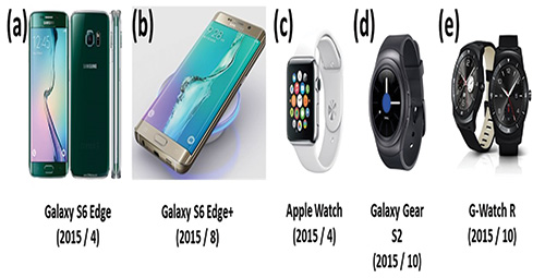
Fig. 1: These commercialized AMOLED products on PI substrates came out in 2015. The AMOLED displays were manufactured by Samsung (a,b,d) or LG (c,e).
Bulk-Accumulation Oxide TFTs
However, a-IGZO TFTs also have challenges. The low yield, non-uniformity, and bias instability of oxide TFTs limit their application to commercial products. In this article, we explain the device concept of a bulk-accumulation (BA) TFT, which has many advantages compared with conventional single-gate TFTs. LCDs use a single TFT to charge the cell to a prescribed voltage. Once the cell is charged, the TFT shuts off and the LCD material is rotated to the correct driven state. The system remains stable for the rest of that refresh cycle because the LC material response to the charge voltage is stored in the cell. In an AMOLED display, however, the TFT (or array of TFTs) must continuously conduct current at a prescribed analog value for the entire frame time. Thus, issues such as the stability and uniformity of mobility matter a great deal.
For an AMOLED display, we need at least two TFTs; one is a switching TFT, which plays the same role it does in LCD switching, and the other is a driving TFT
that is connected in series with the OLED. Therefore, the driving current always has one directional current flow so that the threshold voltage should be stable during OLED operation, but an a-Si:H TFT suffers from defect generation via electron accumulation in the channel when the TFT is on, leading to an increase in the Vth of the driving TFT, and thus dimming the display screen. This is a fundamental issue that cannot be overcome. Therefore, a-Si:H TFTs cannot be applied to AMOLED displays.
Our university’s research teams have made significant progress in overcoming some of these limitations by developing a bulk-accumulation TFT, which employs n-type a-IGZO as its active material, a silicon-dioxide layer as both the gate-insulator and passivation layer, and molybdenum as its metal electrodes [Fig. 2(a)].
A dual-gate TFT has the same device structure as a single-gate TFT,1 using the bottom as the main gate and the top as an additional gate to control
the carrier concentration at the top interface as shown in Fig. 2(a). The transfer curves measured at the bottom gate sweep are shown in Fig. 2(b), where the top-gate potential is controlled from positive to negative. The parallel shift of the threshold voltage is apparent. The electron concentration at the bottom and top interfaces can also be seen, respectively, in Figs. 2(c) and 2(d), and Fig. 2(e) in bulk accumulation.
The concept of BA is that the induced charges by top- and bottom-gate potentials are placed in the bulk and at the bottom/top interface regions of the channel.2 BA is a condition in which the accumulation layer of electrons is not only
confined to the semi-conductor/gate-insulator interface, but extends to the entire depth of the semiconductor (Fig. 2). We need top and bottom gates because the semiconductor layer is thin – gates cannot be covered at the sides of a transistor’s active layer. This is achieved by employing a dual-gate structure in which the semiconductor layer is thin (< 25 nm) and the top gate and bottom gate are electrically tied together [Fig. 2(a)].2
Compared to single-gate-driven TFTs, the benefits of bulk-accumulation TFTs include a drain current that is over three times larger, a turn-on voltage that
is closer to 0 V, a smaller subthreshold voltage swing, better device-to-device uniformity, and better bias and light stability [Fig. 2(b)].3-5 Better stability is attributed to high gate drive and less carrier scattering at the interfaces. Because of the bulk accumulation/depletion, the subthreshold swing is always small, the turn-on voltage is always around 0 V, and device-to-device uniformity is much better than that of single-gate TFTs. The increase in the drain currents is partially due to the higher electron mobility with increasing carrier concentration in the channel, as shown in Fig. 2(f).6
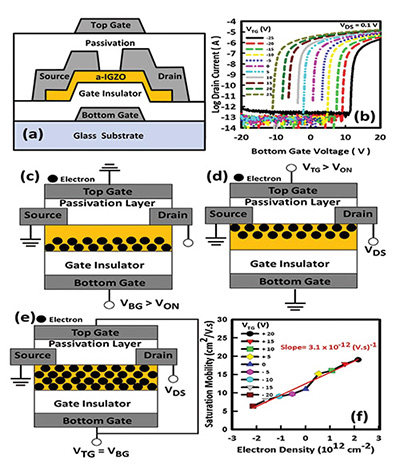
Fig. 2: The structure and characteristics of dual-gate a-IGZO TFTs are shown, including (a) a schematic cross-sectional view of a dual-gate TFT and (b) transfer characteristics measured for VDS = 0.1 V with the bottom-gate (VBG) sweep from –20 to 20 V, while biasing the top gate (VTG) with various constant potentials from –25 to 25 V with 5-V steps. In (c), (d), and (e), schematic cross-sectional views of the electron accumulation region are shown in (c) a bottom-gate sweep, (d) a top-gate sweep, and (e) a dual-gate sweep (BG is electrically tied to the TG). Dual-gate driving results in bulk accumulation when the active layer is thin, whereas in single-gate driving TFTs, the channel is confined to the interface regions. The mobility in the saturation region extracted from the bottom-gate sweep vs. the electron density in the channel induced by the top-gate bias is shown in (f).6
The requirements for the BA TFT are low density of states (DOS) in the gap of AOS because the accumulation depth from the interface decreases with increasing gap state density and also low density of interface states with bottom- and top-gate insulators. Note that most of the induced electrons accumulate at the interface region when the DOS is high. Another important practical condition is active-layer AOS thickness because the area density of the gap states increases with AOS thickness.
Evidence of bulk accumulation can be seen in the output characteristics of dual-gate TFTs measured under three gate modes: bottom gate (sweeping bottom gate, while grounding top gate), top gate (sweeping top gate, while grounding bottom gate), and dual gate (synchronized sweep, in which the top gate is connected to the bottom gate) as shown in Fig. 3(a). Given that dual-gate currents are larger than the sum of the bottom-gate and top-gate currents, the device is governed by bulk accumulation. The experimental evidence of the advantage of BA TFTs is shown in Fig. 3(a), where the currents by dual-gate sweep can be 3–5 times those of single-gate TFTs. The uniformity of the TFT transfer characteristics are compared as shown between Figs. 3(b) and 3(c), where researchers took a bad lot of TFTs to see the clear difference, using a 15 × 15 cm glass substrate and showing a large deviation in the transfer curves for bottom-gate TFTs.
The advantage of BA is shown as the increase of mobility with increasing carrier concentration in the channels of oxide semiconductors.6 The Hall mobility of oxide semiconductors increases with doping concentration, which is quite different from Si and III-V semiconductors, where mobility drops with increasing doping concentration due to impurity scattering by the ionized impurity atoms.
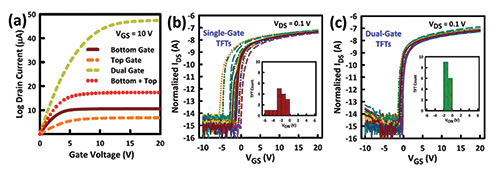
Fig. 3: In (a), the output characteristics of a dual-gate a-IGZO TFT under various gate bias sweep modes is shown. “Bottom Gate” is only the bottom-gate voltage sweep with grounding of the top gate. “Dual Gate” is the gate sweep with the top gate electrically tied to the bottom gate. “Bottom + Top” is the sum of the currents by bottom-gate and top-gate sweeps. Transfer characteristics of 15 single-gate (b) and 15 dual-gate (c) a-IGZO TFTs are shown across a 15 × 15-cm glass substrate with TFTs with a channel width (W) = 20 μm and channel length (L) = 20 μm. Dual-gate TFTs are dual-gate driving. Insets of (b) and (c) are the histograms showing the distribution of the turn-on voltages.2
High-Performance BA Oxide-TFT Circuits
The advantage of BA TFTs can be confirmed by comparing the speed of the ring oscillators made of singe-gate (SG) and BA oxide TFTs. The rise and fall times of an example shift register depend on the performance of the TFT used in the design. Our researchers have confirmed the advantage of BA TFTs through a comparison of
the TFT circuits of a ring oscillator (RO) and the shift register made of SG and BA TFTs. Note that most AMLCD and AMOLED products with IGZO TFT backplanes have the driver ICs bonded in the peripheral area due to inferior TFT uniformity and performance.
Figure 4(a) shows the equivalent-circuit schematics of an inverter (left) and its 11-stage
ring oscillator with output buffers (right). In each inverter stage, the width (W) of the load and driving TFTs are, respectively, 60 and 480 μm with L = 10 μm. Typical output waveforms of SG-driven and BA-driven ROs are, respectively, shown
as symbols in Figs. 4(b) and 4(c) for VDD = 20 V.7 The oscillation frequencies are ~334 and 781 kHz, respectively, for SG driving and BA driving. The RO implemented with BA-driven TFTs oscillates at a higher frequency, the speed of which is comparable to that of ROs based on etch-stopper-type TFT structures.8 Note that the high oscillation frequency exhibited by the BA-driven RO presented herein is achieved at a lower VDD and with the simple back-channel-etched (BCE) process. This is mainly due to two reasons: (1) the μFE under BA driving is higher than that of the SG TFT; (2) the top gates do not introduce additional parasitic capacitance owing to the 2-μm offsets between TG and the source/drain.2,9 The SmartSpice simulation results of the output waveforms (solid lines) of the two types of ROs match well with the experimental results. This good agreement is due to the excellent uniformity of fabricated a-IGZO TFTs and the consistency of their dynamic characteristics with static characteristics.
The speed of a-IGZO TFT-based circuits can be further enhanced by proper circuit design. Figure 4(d) shows a proposed pseudo-CMOS inverter (left) and its 7-stage RO with pick-out buffers (right).10 The advantage of the pseudo-CMOS circuits compared to the ratioed inverters [Fig. 4(a)] can be seen in Ref. 11. Figure 4(e) shows the VDD frequency dependency, including the comparison between pseudo-CMOS-type ROs using SG and BA TFTs with L = 10 or 6 μm. A RO with an L = 6 μm shows faster speed, but both results show much higher speed compared to those of a SG TFT-based RO. This result, therefore, proves that due to the better switching characteristics of BA TFTs, which include higher on-state TFT current and lower switching speed, the switching speed of pseudo-CMOS circuits can also be improved by the
implementation of BA TFTs.
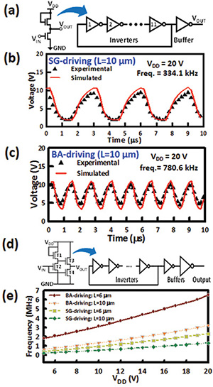
Fig. 4: The comparison of the operational speed of the SG-driving and BA-driving circuit shows (a) equivalent-circuit schematics of a ratioed inverter (left) and its 11-stage ring oscillator (RO). Typical output waveforms include (b) an SG-driven and (c) BA-driven RO at the supply voltage VDD = 20 V. The SmartSpice circuit simulation results in output waveforms (solid lines) of the two types of ROs that match well with the experimental results (symbols). In (d), the circuit schematics of a pseudo-CMOS inverter (left) and its 7-stage RO. (e) shows the output frequency dependency on supply voltage VDD> for SG and BA pseudo-CMOS ring oscillators, with channel length L = 10 or 6 μm.9,10
The shift registers based on SG and BA a-IGZO TFTs were fabricated. Optical images of the fabricated SG and BA shift register are shown, respectively, in Figs. 5(a) and 5(b). Typical output waveforms of SG and BA a-IGZO TFT-based shift registers are, respectively, shown in Figs. 5(c) and 5(d) for a pulse height VH = 20 V.
The current levels of driving TFTs are important because they determine the delay time of the gate driver by taking advantage of the high on-currents in BA a-IGZO TFTs. The rise and fall times are 0.83 and 0.84 µsec for the BA-TFT-based shift register and 1.08 and 1.22 µsec for the SG-TFT-based shift register, respectively. It is well known that parasitic capacitance slows down dynamic operation. Here, the top gate does not introduce additional parasitic capacitance (between TG and S/D), due to the 2-μm offsets. Low-level-holding TFTs require good stability under positive-bias stress, given that they are mostly in on-state to maintain the voltage at node Q and output at low during the low-level holding period. However, BA a-IGZO TFTs have been reported to be very stable under positive-bias stress, which indicates a higher yield and longer lifetime. In addition, BA-TFTs give better turn-on voltage (VON) uniformity compared to that of SG-TFT.5 Because of bulk accumulation/depletion, the TFT VON is always close to 0 V, indicating an enhancement-mode operation, which allows the realization of simple shift-register circuits without the necessity of level shifting or additional low-level signals.
We have confirmed that BA-TFTs with a TG offset structure enhances the speed and lifetime of the shift register5 through advantages such as high ION and a small sub-threshold swing (SS). We were then able to further reduce the pitch (width) of the BA-TFT-based shift register. Earlier, we had reported a 30-µm-pitch gate driver.12 The single stage is small in physical size – only 720 × 30 µm – much smaller compared to other oxide-TFT-based gate drivers reported in the literature. Figure 5 (bottom) shows the output waveform of the gate driver for an input pulse VH of 20 V with a pulse width of 2 µsec. The high-output voltage and rise and fall times are, respectively, ~19.7 V, 583 nsec, and 617 nsec.
To this point, we have described the attributes and benefits of BA oxide-TFT backplanes. In part II of this article, we will describe a flexible AMOLED display with integrated gate drivers using BA-oxide TFTs that is demonstrated with a carbon-nanotube/graphene oxide (CNT/GO) buffer embedded in a plastic substrate.
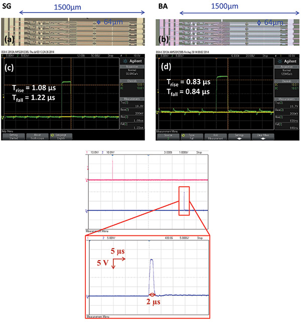
Fig. 5: (a) and (b) are the optical images and (c) and (d) are typical output waveforms for SG and BA a-IGZO TFT-based shift registers, with (a) and (c) for SG and (b) and (d) for BA TFTs. At bottom are output waveforms of the BA shift registers for 30-um gate drivers
with a pulse height of 20 V with a width of 2 µsec.12
References
1M. J. Seok, M. H. Choi, M. Mativenga, D. Geng, D. Y. Kim, and J. Jang, “A full-swing a-IGZO TFT-based inverter with a top-gate-bias-induced depletion load,” IEEE Electron Device Letters 32(8), 1089–1091 (2011).
2M. Mativenga, S. An, and J. Jang, “Bulk Accumulation a-IGZO TFT for High Current and Turn-On Voltage Uniformity,“ IEEE Electron Device Letters 34(12), 1533–1536 (2013).
3S. Hong, S. Lee, M. Mativenga, and J. Jang, “Reduction of negative bias and light instability of a-IGZO TFTs by dual-gate
driving,“ IEEE Electron Device Letters 35(1), 93–95 (2014).
4S. Jin, T.-W. Kim, Y. Seol, M. Mativenga, and J. Jang, “Reduction of positive-bias-stress effects in bulk-accumulation amorphous-InGaZnO TFTs,“ IEEE Electron Device Letters 35(5), 560-562 (2014).
5S. Lee, M. Mativenga, and J. Jang, “Removal of negative-bias-illumination-stress instability in amorphous-InGaZnO thin-film transistors by top-gate offset structure,“ IEEE Electron Device Letters 35(9), 930–932 (2014).
6M. Chun, M. D. H. Chowdhury, and J. Jang, “Semiconductor to metallic transition in bulk accumulated amorphous
indium-gallium-zinc-oxide dual gate thin-film transistor,” J. Appl. Phys. 5, 057165/1-6 (2015).
7X. Li, D. Geng, M. Mativenga, and J. Jang, “High-speed dual-gate a-IGZO TFT-based circuits with top-gate offset structure,” IEEE Electron Device Letters 35(4), 461–463 (2014).
8D. Geng, D. H. Kang, and J. Jang, “High-performance amorphous indium-gallium-zinc-oxide thin-film transistor with a self-aligned etch stopper patterned by back-side UV exposure,” IEEE Electron Device Letters 32(6), 758–760 (2011).
9X. Li, D. Geng, M. Mativenga, Y. Chen, and J. Jang, “Effect of bulk-accumulation on switching speed of dual-gate a-IGZO TFT-based
circuits,” IEEE Electron Device Letters 35(12), 1242–1244 (2014).
10Y. Chen, D. Geng, M. Mativenga, H. Nam, and J. Jang, “High-speed pseudo-CMOS circuits using bulk accumulation a-IGZO TFTs,” IEEE Electron Device Letters 36(2), 153–155 (2015).
11T.-C. Huang et al., “Pseudo-CMOS: A design style for low-cost and robust flexible electronics,” IEEE Trans. Electron Devices 58(1), 141–150 (2011).
12D. Geng, Y. F. Chen, M. Mativenga, and J. Jang, “30-μm-Pitch Oxide-TFT-Based Gate-Driver Design for Small-Size, High-Resolution, and Narrow-Bezel Displays,” IEEE Electron Device Letters 36(8), 805–807 (2015). •
Jin Jang is the director of the Advanced Display Research Center and Department of Information Display at Kyung Hee University in Seoul, Korea. He can be reached at jjang@khu.ac.kr.