Developing a 110-in. 4K × 2K TV
Developing a 110-in. 4K × 2K TV
China Star has demonstrated a 110-in. LCD TV that has an outstanding dynamic contrast ratio of 50000:1, ultra-high brightness of 1000 nits, high-saturated color reproduction, and a 288-zone local-dimming backlight. Manufacturing a high-definition high-quality TV in such a large size brings with it special manufacturing challenges.
by Li-Yi Chen, Yu-Yeh Chen, Hung-Lung Hou, Yuming Mo, and Chung-Yi Chiu
RECENTLY, China Star Optoelectronics Technology Company (CSOT) successfully developed a 110-in. UHD (3840 × 2160) 3-D TFT-LCD TV panel. It was the world’s first LCD panel to offer 4K × 2K resolution and 3-D capability. The maximum brightness of the panel is 1000 nits, achieved with less than 1100 W of power consumption via an LED backlight with local dimming. The color gamut is much larger than that of traditional LCD TV panels, with vivid primary colors due to the use of LED backlighting. The static dark-ambient contrast of the panel is greater than 4000:1. The panel’s 3-D display technology uses 120-Hz shutter-glasses technology, and the large size particularly enhances viewer enjoyment of 3-D movies and games.
The goal for making this 110-in. panel was to provide a powerful sense of immersion and “reality” for the viewer. One of the most important enabling aspects for this capability is the visual angle. Studies have shown that a larger visual angle will provide a more immersive experience.1,2 From the same distance, a bigger panel obviously can provide viewers with more information presented over a wider visual angle, as Fig. 1 illustrates. The visual angle increases by two times when the panel size increases from 55 to 110 in.
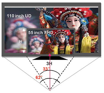
Fig. 1: The viewing angle from the same distance increases with the size of the panel.
At the same time, resolution must be increased to maintain high visual quality with larger visual angles. For example, 1920 pixels spread over a wide visual angle or over a long horizontal distance and then viewed from close range results in a poor visual experience because of the low number of pixels per inch . Of course, people tend not to sit quite this close to large TVs. Even so, in a living room where the space is fixed, a larger panel with high
resolution and optimal viewing angles will provide the best viewer experience. When presented on a larger display such as one that is 110 in., full HD (FHD) does not satisfy what people expect to see in terms of imagery. Increasing the pixels per inch improves the picture performance and thus provides a better stereoscopic experience.
Manufacturing and Technology Challenges
The 110-in. panel was fabricated in a newly established Gen 8.5 fab by CSOT. There were many manufacturing challenges. Both for the TFTs and color-filter substrates, it was necessary to use multiple photolithography exposures (shots) to define the images in each mask step (Fig. 2). These multiple shots build up a patchwork quilt of the full array pattern for each step. A typical mask and panel pattern is shown in Fig. 3. Shot mura is caused by a variation of the critical dimensions in patterns and indirectly affects optical performance. For example, in the black matrix, the aperture of the pixel area controls the ratio of light transmittance. If the black-matrix dimensions change, the display luminance in that area will also change. This is especially true if the mura is located at the boundary of each unit shot in the mask. When the entire panel pattern is assembled with each unit shot in the mask, the boundary of each shot will be exposed twice because of the misalignment of the mask system. Similarly, if the two shots do not align perfectly, then the boundaries between
the shots will produce a pattern that is not consistent with the rest of the regions (Fig. 4). The resulting dimensions of the black matrix may then be different between the inside region and the boundary of each shot. CSOT has developed special proprietary photo recipes to solve this problem.
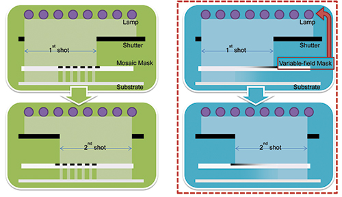
Fig. 2: Two exposure systems are shown: the mosaic (left) and variable-field (right).
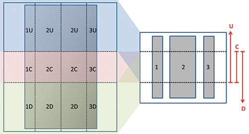
Fig. 3: Typical mask and panel patterns are shown.
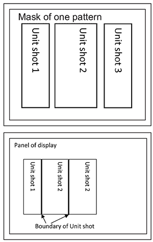
Fig. 4: Shot mura is particularly troublesome at the boundaries.
RC loading is a term that describes the combination of parasitic capacitance and series resistance in each TFT lectrode. The larger these values, the longer it takes to establish a stable voltage level on the electrode. As the display size increases, both of these parameters also increase. To put this in perspective, consider the example of a full-HD (1920 × 1080) 55-in. LCD panel being driven at a 120-Hz frame rate. This requires a charge time on each gate of less than 7.5 µsec. With today’s driver, interconnect, and line fabrication technology, this charge time can be easily achieved with some degree of design margin included. In fact, the settling time due to the RC effects is around 2 µS. However, if the resolution is only doubled in the preceding example, the available charge time is cut in half and the voltage levels on each line will not reach a stable value in time to charge the TFT cell to the correct data value. If the dimensions of the panel in each axis are then increased to roughly twice those of the 55-in. panel, the parasitic capacitance and line resistance is effectively doubled, creating an even greater challenge in achieving acceptable charge levels in each pixel cell. The settling time alone of a 110-in. 4K × 2K panel is about 8 µS. Therefore, a more innovative driving scheme was developed to overcome this limitation: the hG2d driving design.
Pre-Charging Driving Scheme
Decreasing the amount of gate drivers by half and doubling the data (hG2D) driving was the first method considered to extend the charging time.4,5 Compared with a normal 60-Hz panel, hG2D (source) drivers are used. Also, gate and source dual-side inputs were implemented in the architecture to reduce the loading impact, as shown in Fig. 5. Based on the current specifications of the IC and driver, 120 Hz with FHD is a better design. For the current Al process used, a charge time of 7.5 µsec is required for an 80-in. panel. However, if the frame rate is increased or the resolution doubled, the charge time is halved. Therefore, it is necessary to reduce charge time by using other methods. One approach is to turn on more than one gate at a time. When two gates turn on simultaneously, two sources of data information into the pixels are needed. Hence, the dual-data-line design with a pattern is needed in one pixel. This arrangement consists of half the gate input and twice the data input in one pixel. There are still some issues with this driving scheme and the picture performance for very large LCDs.
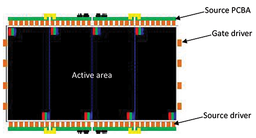
Fig. 5: This gate/source dual-driving setup was used for the 110-in. panel. Source PCBA: Transmits all display data and control signals from the control board to the
source driver IC. Source Driver: Receives display data and converts digital signal to analog voltage for driving the TFT-LCD device. Gate PCBA: Transmits all gate driver control signals from the control board to the gate driver IC. Gate Driver: Controls scan line to turn on/off the TFT device line by line sequentially.
For an ideal initial setting of the driving waveform as shown in Fig. 6(a), the pixel voltage needs to be at a desirable value. For the ideal case, the pixel voltage should be charged rapidly to the correct value. However, the circuit resistor or capacitor usually causes distortion in this charging on the rising and falling edges. Thus, if the charging time is insufficient, the pixel voltage will not be correct. With Vft = ΔV1, insufficient charge flows to the LC capacitor. When this circuit scheme was used for the 110-in. LCD, the researchers encountered an enormous obstacle in charging uniformity. The distortion depends on accumulated parasitic capacitance and LC capacitance through the panel.
After propagating a distance to get to the cell, the gate and data waveforms change and overlap the undesirable area of the next target voltage, which is different from the initial setting as shown in Fig. 6(c). Hence, the target pixel voltage is difficult to achieve and suffers a voltage drop of ΔV3, including a lack of carrier charging, feed-through voltage, and error charging
to the next target voltage. To overcome this difficulty, the pre-charge concept was utilized to inject enough carriers into the LC capacitance and suppress the error charging ratio by overlapping the next target voltage.
Figure 6(b) and 3(d) depict the pre-charging setting. It is apparent that ΔV4 is compensated and is smaller than ΔV3. Meanwhile, ΔV2 and ΔV4 can be modified and are almost the same as ΔV1. This structure allows for an extension of the charging time and a reduction of the gate-delay influence. Figure 7 shows a schematic for gate output with and without pre-charging.
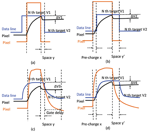
Fig. 6: A driving waveform is depicted with normal and pre-charge schemes. Image (a) shows an ideal waveform, (b) shows the same waveform in pre-charge mode, image (c) shows a normal setting, and (d) shows the pre-charge mode.
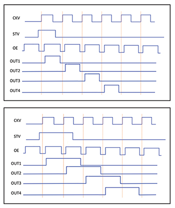
Fig. 7: On the top is the gate output charge for the waveform without pre-charging. On the bottom is the gate output charge with pre-charging. The duration of higher times should be extended. The longer charging time will overcome the lack of pixel voltage.
Figure 8 shows some quality issues caused by error charging. At the left of the image of the man’s mouth in Figure 8(a), there is a rough edge around the lips, which is the result of error charging. Optimizing the timing between gate and data pulse as illustrated in Figs. 6(b) and 6(d) helps to improve this phenomenon, as shown in Fig. 8(b). After optimization, it was possible to retain the well-charged performance and avoid error charging at the same time. The result was an improvement in available charging time to 15.4 μsec, which overcame the limitations due to the RC loading.
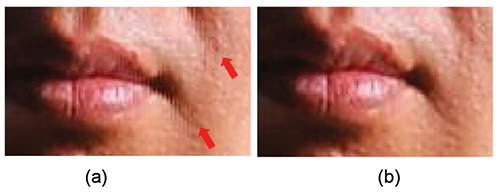
Fig. 8: The image at left (a) shows degradation due to error charging. The image at right (b) demonstrates that this has been eliminated through pre-charging modification.
UHD System Architecture
Recently, UHD systems have been in demand for high-resolution applications. Technical concerns include the bandwidth of the architecture and the data transmission of the display port. Essentially, this technology has not matured enough for commercial applications, and many system makers are still trying to integrate the hardware and software.
The major initial concerns for a 4K × 2K display are transmission line loading and image process bandwidth. Hence, a panel is usually divided into four units (1920 × 1080 by each unit) to overcome the difficulties of the panel, field-programmable gate array (FPGA), and graphics card, as shown in Fig. 9(a).
One common problem with the approach in Fig. 9(a) is that a block boundary can often be observed in the image along the center cross on the panel. The vertical boundary results from the time delay between the dual-DVI ports. The image is detected as a space shift along the center line. The horizontal boundary is caused by the signal difference of the data line. As mentioned above, the researchers adopted an FPGA (Stratix series from ALTERA) to synchronize the graphic card (from AMD) and the 110-in. panel as shown in Fig. 9(b). The cell is designed with double-sided gate/data driving to minimize the distortion caused by the RC delay. Under a specified algorithm in the FPGA, the resolution of each unit becomes 1920 × 2160, which is synchrocontrolled by opposite control boards, referred to as C/B-A and C/B-B. For commercial applications, the 110-in. 4K × 2K panel is also capable of 3-D functionality at 120 Hz.
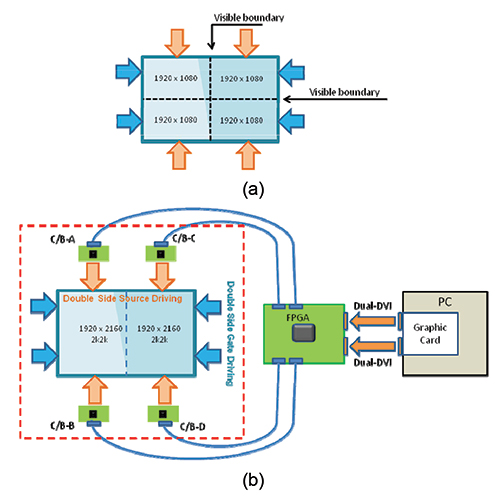
Fig. 9: Shown is (a) a diagram of a popular current panel driving concept and (b) the proposed alternate architecture for a UHD system.
Advanced Mura-Free Technology
Because the 110-in. panel size was larger than the photomask size on the Gen 8.5 production line, it was not possible to complete the production of the entire panel by using only one shot. Stitching-mask technology was therefore used in the development.
As is well known, controlling the uniformity of stitching areas is extremely difficult. Uniformity issues or mura often appear as a result of multiple time exposures at the shot stitching point.
In the early stages of the project, the shot mura could be easily seen on the panel. After the researchers fine-tuned the process parameters, the shot mura was greatly reduced. In Fig. 10, reduction of shot mura is apparent in the middle of the image on the right.
Besides process optimization as mentioned above, another solution uses algorithm adjustment in the graphics engine. This system compensation was also developed and adopted for mura suppression in critical areas. The adjustment flow, or “de-mura” function, is a software-based approach to fine-tuning the gray levels of the panel in the areas where there is mura that cannot otherwise be fixed as depicted in Fig. 10.
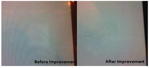
Fig. 10: Shot mura reduction can be seen in the image at right (center of image).
Based on this algorithm with FPGA coding, the panel demonstrated improved performance, as shown in Fig. 11.
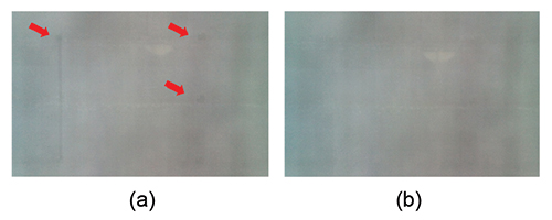
Fig. 11: Panel performance is depicted before (a) and after (b) algorithm adjustment.
3-D Stereoscopic Technology
3-D functionality was incorporated into the 110-in. LCD by using the L-R field-sequential method combined with active shutter glasses.
In order to prevent crosstalk, the designers had to adjust the turn-on sequence of the backlight to minimize the ratio of overlapping. Based on a direct-type LED backlight, they utilized a vertically scanning backlight consisting of 16 sections to improve the 3-D performance. After optimized sequences between the LED backlight, glasses and LCD, a
crosstalk performance of 2.5% could be achieved with a comfortable visual quality. Changes in the detailed gray levels with a fixed right-eye observation and left-eye patterns resulted in good uniformity, as shown in Fig. 12.
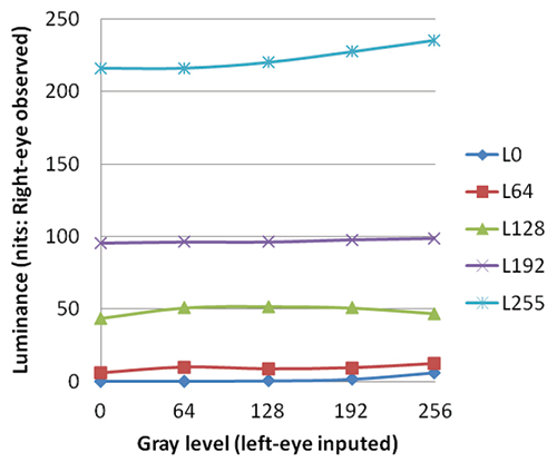
Fig. 12: 3-D luminance stability (crosstalk) is shown with gray-level switching.
Creating a 110-in. UHD LCD TV Table 1 summarizes the main characteristics of the UHD LCD TV. A 110-in. panel with such high performance is a significant achievement. The brightness can exceed 1000 nits, the resolution is four times that of standard HD, and the TV has extremely real-istic color reproduction. This large-size and high-resolution technology was made into a commercial
product that is vailable now from several Chinese retailers. (The TV won the Society for Information Display’s Display of the Year Silver Award for 2013.) CSOT hopes that it has created a completely new viewing experience that
establishs a brilliant landmark for LCD-TV technology in particular.
Table 1: The TV’s main parameters are shown.
| Specification |
Output |
| Diagonal screen |
110” |
| Frame rate |
120 Hz |
| Resolution |
3840 x 2160 (R/G/B) |
| Brightness |
1000 nits |
| Color coordinate |
(0.275, 0.28) |
| Contrast |
4200:1 (Static)
50000:1 (Dynamic) |
| Color saturation |
92% |
| View angle |
178°/178° (H/V) |
| Gray to gray |
6.5 ms |
| 3D crosstalk |
2.5% |
References
1M. Sugawara, K. Masaoka, M. Emoto, Y. Nojiri, and F. Okano, “Super-Hi-Vision — An Ultra-High Definition Television and Its Human Factors,” IMID/IDMC ’06 Digest, 81–85 (2006).
2M. Sugawara, K. Masaoka, M. Emoto, Y. Matsuo, and Y. Nojiri, “Research on Human Factors in Ultrahigh-Definition Television (UHDTV) to Determine Its Specifications,” SMPTE Mot. Imag. J. 117, no. 3, 23–29 (April 1, 2008).
3S-S. Kim, B-H. You, J-H. Cho, S-J. Moon, B. H. Berkeley, and N. D. Kim, “An 82-in. Ultra-Definition 120-Hz LCD TV Using New Driving Scheme and Advanced Super PVA Technology,” SID Symp. Digest Tech. Papers, 196–199 (2008).
4B-H. You, J-S. Bae, D-W. Park, S-Ha Hong, S. Saito, and J. T. Moon, “UD Resolution 240Hz LCD TV Display System with High Speed Driving,” SID Symp. Digest Tech Papers, 395–398 (2012).
5B-H. You, J-P. Lee, D-G. Kim, K-Ho Park, Y-J. Kim, B. H. Berkeley, and S. S. Kim, “A Novel Driving Method Using 2-Dimension Spatial Averaging for High Speed Driving of AMLCD,” SID Symp. Digest Tech. Papers, 1275–1278 (2007). •
Li-Yi Chen, Yu-Yeh Chen, Hung-Lung Hou, Yuming Mo and Chung-Yi Chiu are with China Star Optoelectronics Technology Company, Ltd, Shenzhen, Guangdong, China. Y-Y Chen can be reached at Cyychen@tcl.com.