New Transparent Conductors Take on ITO for Touch-Screen and Display Applications
New Transparent Conductors Take on ITO for Touch-Screen and Display Applications
Indium tin oxide (ITO), a transparent conductor, has been a staple of flat-panel display manufacturing for decades and has been in great demand from the growing touch-screen industry. Limitations of cost and performance, as well as concerns over availability, have led to the search for a replacement material. Several candidates exist or are in development, but none have yet gained the scale to displace ITO.
by Paul Semenza
TOUCH screens, LCDs, thin-film solar cells, and other devices require the creation of electrodes on a substrate (usually glass or plastic film) that are both transparent, so as not to block light through or from the display or to the photovoltaic material, and highly conductive, to optimize power consumption and sensitivity. As if finding a material that can provide optical transparency and electrical conductivity were not challenging enough, flexibility (as in bendability), ease
of manufacturing, and, of course, low cost are also requirements.
ITO: Challenged, But Still the Dominant Transparent Conductor
The material used for the vast majority of transparent conductors is indium tin oxide (ITO, typically 90% In2O3 and 10% SnO2 by weight). ITO is the most prevalent example of the class of transparent conductive oxides,
which can also include nitrides or fluorides (e.g., TiN), as well as ZnO and CdO. Doped oxides include In2O3:Sn (ITO), ZnO:In (IZO), ZnO:Al (AZO), ZnO:Ga (GZO), and SnO2:F (FTO); mixed oxides include In2O3–ZnO, CdIn2O4, and Zn2 SnO4.
Indium is a rare-earth metal, typically extracted as a by-product of zinc or tin mining. As such, there have been supply and pricing concerns. Supply concerns have been alleviated to some extent by the development of new mines and recycling, but given the concentration of mines, political conflicts, such as that in 2012 between China and Japan over the East China Sea, have the potential to threaten supply. Indium pricing has also been highly dynamic, ranging from $200 to $1000/kg;
recent prices have been around $500/kg.
The manufacturing process for ITO also impacts costs. Magnetron sputtering, the process typically used for ITO deposition, can involve material wastage of more than 50% and is energy intensive. The temperatures needed for crystalline alignment of ITO film are close to the melting point (250°C) of PET, the most common film. Some ITO film makers are developing transfer methods to improve efficiency.
In addition to cost and manufacturing issues, ITO has performance limitations. ITO is transparent, but often has a yellow tint. Its refraction index is 2.0 (depending on the process and density), which is higher than glass (1.4) and PET (1.4–1.6), and means that high reflection values are commonly encountered and even
total internal reflection of passing light is possible. To increase conductivity, increased film thickness is used, which can result in etching marks. Finally, ITO is brittle and subject to cracking, especially under conditions in which the film is actively flexed, but can also crack due to stretching during
the patterning or lamination process, especially with ITO film.
Despite the cost and performance limitations, ITO is the dominant form of transparent conductor and has an established supply chain, including targets, sputtering, substrate, and patterning processes. As shown in Fig. 1, ITO film capacity was over 20 million m² in 2012 and will increase by a third in 2013. Because of the high volume of flat-panel displays and touch screens that demand transparent conductors, replacing ITO requires stable and qualified material sources and mature supply chains, including deposition (coating) and patterning processes.
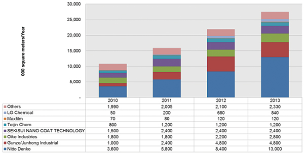
Fig. 1: ITO film capacity is expanding to meet the increased demand for touch screens (Source: DisplaySearch Touch Sensor Market and Evolution Report, 2013).
Several New Materials Vying to Replace ITO
Several different approaches are under development for the mass production of high-performance transparent conductors at low cost. Rather than using transparent oxides, these approaches tend to utilize advanced processing of common materials such as silver or advanced materials such as polymers or nano-tubes. Each of these approaches has features and limitations (Table 1); in addition, the level of process maturity and supply chain also vary greatly.
Table 1: New transparent conductors with the potential to replace ITO are being pursued by many companies. (Source: DisplaySearch Touch Sensor Market and Evolution Report, 2013).
| Material |
Pros |
Cons |
Makers |
| Metal Mesh |
Low resistance: 0.1-30 Ω/sq. |
Mesh can be visible and interfere with LCD pixels (moiré patterns); surface roughness is bad for OLED, PV; long design time |
3M, Atmel, CIT, Fujifilm, Gunze, NanoGrid, PolyIC, UniPixel, Fujimori |
| Silver Nanowire; Nanoparticle |
High conductivity/transparency; easy to use, inexpensive; established supply chain |
Increased haze <30 Ω/sq. |
Blue Nano, Cambrios, Carestream Carestream, Ferro, Saint-Gobain, Seashell, SVG; Cima NanoTech |
| Conductive Polymer |
Inexpensive, solution coating |
Low conductivity at acceptable transmission (resistance >100 Ω/sq.); bluish color; reliability affected by humidity |
Agfa, Daicel, Heraeus, Kodak, Lintec, Nagaoka Sangyou, Oji, TDA Research |
| Carbon Nanotube |
Robust and stable |
Low conductivity at acceptable transmission (resistance >100 Ω/sq.); hard to wet-etch |
C3Nano, Canatu, Eikos, LG Chem, Mitsui, SouthWest NanoTechnologies, TECO, Top Nanosys, Toray, Unidym |
| Graphene |
Stable, reliable; bendable/foldable |
Still in R&D stage |
Bluestone, Graphene Square |
In addition to a stable supply chain, new materials must prove that they are superior to ITO in performance. There are several important factors in determining which materials can reasonably challenge ITO. Requirements for touch sensors include electrical conductivity, optical transmittance, material stability, and mechanical features (such as bendability and flexibility).
Metals are excellent conductors, of course, but not generally transparent. However, transparency can be achieved through the use of very thin (<10 nm) foils or by using certain patterns or structures. A metal mesh can be made from highly conductive metals such as copper or silver with very fine lines or particles (<5 µm is not visible to human eyes) in a grid pattern. If the metal lines make up 1% of the area, it is possible for the grid to have high transmittance. The electrical conductivity is related to the grid density or line thickness and can be less than 50 Ω/sq. for notebook PC sizes. Line widths of 10–20 µm are typical, with gaps of several hundred microns. The regularity of the grid pattern in metal-mesh touch sensors can lead to diffraction (moiré) patterns when overlaid on a display with a regular pixel structure, particularly when the display is >300 ppi, so the metal-mesh pattern is often rotated at an oblique angle.
Instead of the grid pattern of metal mesh, nanowires have a random alignment. The diameter of nanowires is 20–100 nm; thinner wires enable higher transmittance but are more difficult to make. The density of nanowires decides the sheet resistance (higher density results in lower resistance). Copper (approximately $10/kg) is much cheaper than silver ($800–1000/kg – and silver nanowire ink is about 10 times that of silver), but copper nanowire in ink solution has a much higher production cost. Silver nanowire has excellent conductivity, transmittance, and flexibility. Silver nanowires or nanoparticles can be formulated by AgNO3 reduction, a form of ink.
Organic materials, including conductive polymers, carbon nanotubes, and graphene, can also be used for transparent electrodes. Conductive polymers are not as conductive as metal and ITO but they are easier to process and have lower material costs. In addition, their drying temperatures and other features make them more widely applicable to industrial uses. The most well-known conductive polymer is PEDOT (poly-3,4-ethylenedioxythiophene), which was invented by Bayer and commercialized under the name Baytron. While some conductive polymers can appear dark, PEDOT is light bluish (on the substrate) so that it is more suitable for use as for transparent conductive electrodes. Other conductive polymers are polypyrrole, polythiophene, and polyaniline.
Carbon nanotubes (CNTs) are allotropes of carbon (others are graphite and diamond) formed by atoms combining into tubular hollow cylinders, each one ~1 nm in diameter and 1,000–10,000 times as long. The single-wall format is a single layer; multi-wall is a nest-like structure in which smaller tubes are included in a bigger tube. In addition to the tube form, there are variations such as Canatu’s nanobud, which looks like a tube with fullerene units on it. CNTs offer good optical and electrical performance. Flexibility and stability are excellent because of strong carbon atomic bonding. Generally, CNTs used for touch sensors look somewhat dark, and the sheet resistance is higher than ITO.
Graphene is a single layer of carbon atoms bonded in a hexagonal honeycomb crystal lattice. It has low light absorption (2.3%), high mobility (2 × 105 cm2/V-sec; silicon is 1400 cm2/V-sec), and low resistivity (1.0×10⁻⁸ Ω-m, lower than silver). However, its mass-production process and scale are not mature. Exfoliation has been shown to be effective, but it cannot be applied in large areas. Another method is to grow it on a metal substrate (Ni or Cu) using a process and transfer it to a film substrate.
Metal mesh and silver nanowire have started to be adopted in touch sensors, but the competition is only beginning. Material costs generally depend on production scale and generation method, and the coating or deposition method and patterning process have significant impact. In particular, the patterning process affects the desired touch-sensor specifications; for example, etching/silk printing is cheaper but still cannot compete with photo-lithography because the bigger line/space pitch cannot create narrow bezel designs. Ink-jet printing can achieve line widths < 10 µm and can combine coating and patterning, but only over small areas.
Don’t Count ITO Out Yet
It is likely that ITO replacement materials will make an initial impact in large touch screens for notebooks and all-in-one PCs because cost is critical in these applications, and ITO provides good cost/performance in smaller touch panels and displays. Metal-mesh and silver nanowire/nanoparticle approaches have begun to compete for ITO replacement, and it is likely that other solutions will come to market soon. However, it is too early to declare that one or more of these approaches will significantly displace ITO; for that, material supply and production systems need to be developed to serve markets in the hundreds of millions of square meters. If one or more of these approaches can, in fact. be mass-produced at low cost, it is likely to enable a host of new applications for touch screens, as well as lower the cost of flat-panel displays. •
Paul Semenza is Senior Vice President with NPD DisplaySearch. He can be reached at paul.semenza@displaysearch.com