The Future Is Paper Based
The Future Is Paper Based
Paper may be the key to an entirely new class of inexpensive flexible electronics, including displays.
by Rodrigo Martins, Luis Pereira, and Elvira Fortunato
PRINTED-PAPER ELECTRONICS, with their promise of low cost, flexibility, and full recyclability are attracting more and more interest among product developers. The paper industry today is facing challenges from electronic books and journals. At the same time, the packaging industry is working to develop packaging that can interact with end users. The former is challenged to find alternative sources of revenue and the latter to expand product capabilities. Thus, we are observing a number of companies that are developing paper not only as a surface on which to print ink but also as a surface for electronics. The end result may be a plethora of low-cost disposable and recyclable products.
Examples of current paper-electronics developments from paper and packaging companies include Portucel (Portugal),1 which is developing new types of paper for a broad range of applications, including transparent paper; Felix Scholler (Germany),2 now developing paper for printing electronics as part of a next-generation sustainable paper project based in Europe called A3ple3 Suzano (Brazil),4 which is now researching and developing new papers for electronics applications; and Stora Enso (Finland),5 currently developing new smart packaging. In Korea, there is also a growing interest in promoting the use of the traditional bark-based Hanji paper for other purposes, including electronics.
Indeed, electronic products printed on paper could transform labelling, packaging, and publishing as we know them today, to mention just a few examples. Applications might include intelligent packaging, richer security documents, and inexpensive and flexible diagnostic products for the medical and pharmaceutical industries. Imagine a sheet of newspaper in the form of a rollable and foldable display, which can store information in memory and could incorporate a self-powered
energy unit. The paper of the future could serve as a functionalized electronic component with which we can fabricate our own ergonomic and disposable green phones and products such as lighting woven into paper pulp, cardboard that folds into a box at the touch of a finger, or a paper sheet on which we can play a movie.
In addition, paper is one of the cheapest and most commonly used materials in our society. Cellulose, on which paper is based, is the Earth’s major biopolymer and is of tremendous global economic importance, especially in Europe, which is responsible for 30% of the world’s total production. Paper is also recyclable and so paper-based electronics will help reduce the environmental impact of “electronic trash.”
Some promising paper-based applications have already been demonstrated, including solar cells, displays, capacitors, actuators, gas sensors, magnetic devices, and batteries.6 In all of these applications, however, the paper has a passive function since it is used as a substrate (Fig. 1). It does not take an active role in the device’s working principle. What we are now proposing, in order to achieve the above-mentioned applications, are new disruptive and sustainable paper-based platforms for electronics that not only integrate discrete devices but also use the cellulose as an electronic material for insulators, electrolytes, conductors, and semiconductors. Such a platform is outlined in Fig. 2.
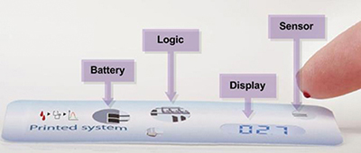
Fig. 1: Paper is the substrate for this smart system that incorporates a printed display. This concept shows how different materials can be printed to integrate different devices, such as a battery, a biosensor, a display, and electronic circuits in the same paper substrate to build a self-sustained bio-detection system. Adapted from blogs.rsc.org.
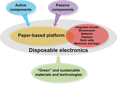
Fig. 2: A novel paper-based platform for electronics includes ICs, batteries, and displays.
Key Materials and Processes
The benefits of paper-based electronic devices and systems were highlighted in the previous section. Achieving these devices imposes some challenges with regard to the necessary materials and processes. One of the first steps toward the use of paper for electronics is to see how conductor lines behave on paper7 when compared to other polymer-based substrates. This has been shown to be possible with nice downward scalability (below 50 µm), as depicted in Fig. 3.
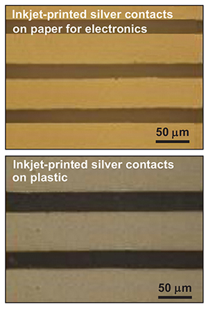
Fig. 3: Ink-jet-printed silver contacts on paper (top) and polymer (bottom) show that scalability and resolution are similar for both types of substrates when printing is used to process conductive lines.
Paper itself can also be used as an active part on some devices. The proof of concept of using paper as an electrolyte has been explored, mainly for battery8,9 and memory10 applications (Fig. 4). The use of paper as a dielectric in producing thin-film transistors (TFTs) has been also demonstrated, using inorganic11–14 or organic15 based functionalized materials. In the first case, the paper is sandwiched between the gate electrode on one side. The channel, with the corresponding drain and source, is placed on the other side of the paper sheet. In the second case, the transistor is organic based and is implanted in an electrolyte gel foil (Fig. 5).
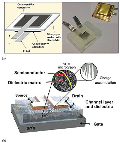
Fig. 4: Image (a) shows a schematic and photo of a paper-based battery.8,9 Image (b) is a schematic of a paper-based memory device based on a floating gate TFT.
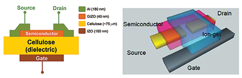
Fig. 5: A paper-based inorganic TFT.11 schematic appears in (a); image (b) depicts a design for an organic TFT on paper.15
These developments, and the ability to make n- and p-type TFTs on paper,16 open the possibility of integrating paper-based TFTs as a core component to build up complementary metal oxide semiconductors (CMOS),17 themselves core components for low-power-consumption analog and digital circuits. This, in turn, opens the door to new applications ranging from smart labels and sensors on clothing and packaging to electronic displays printed on paper pages for use in newspapers, magazines, books, signs, and advertising billboards.
The holistic approach of merging low-power circuitry with a recyclable substrate poses an important step toward greener electronics. The proof of concept developed by our research group, in close cooperation with Professor Arokia Nathan and his group from Cambridge University, UK, shows the possibility of processing CMOS-based electronics (at almost macroscopic scale) with reasonable gains and the ability to scale down either by printing or by using soft patterning techniques (Fig. 6).
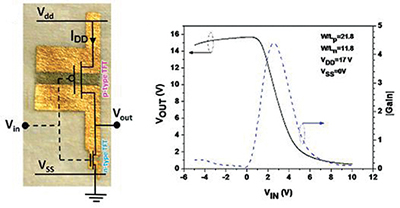
Fig. 6: An image of the configuration of the CMOS inverter on paper (a) appears next to a chart (b) showing its transfer charcteristics and gain.
We can therefore predict the use of these devices as amplifiers, with a common source and differential structure, or integrated as logic gates, such as NOR or
NAND gates (Fig. 7).
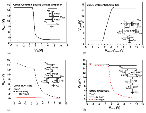
Fig. 7: The above charts depict circuits for electronics on paper including (a) common source amplifier, (b) differential amplifier, (c) NOR gate, and (d) NAND gate.
As far as digital circuits are concerned, we have recently proven the concept18 of creating a variety of simple analog and digital circuit devices such as inverters and flip-flops on paper. These are the building blocks for larger scale circuits such as multiplexers, shift registers, ring oscillators, and others.
Another relevant issue concerns a recent demonstration of the possibility of producing p-n based cellulose made of two oppositely charged microfibrillated cellulose (also known as nanocellulose) sublayers19 (Fig. 8). The current rectification ratio is around 15 at ±5 V and exhibits good repeatability at room temperature. Instead of forming a depletion region to rectify current, this paper diode uses asymmetric charge distribution to selectively control the ion-diffusion direction. The asymmetric charge distribution inside the diode paper can selectively transport cations and anions under positive and negative bias, to allow an electric current to pass in one direction while being blocked in the opposite direction. Although the mechanism is quite different from that of a emiconductor-based p-n junction, the phenomenon turns out to be very similar.
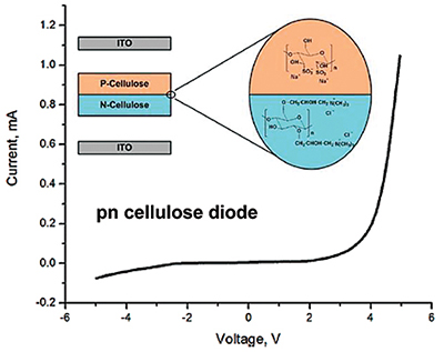
Fig. 8: This chart depicts an I–V curve of a pn junction based on functionalized and doper fibers, all embedded on paper.
Paper-Based Biosensors and Displays
Based on the above examples, we can clearly envision a new type of technology in which the breakthrough idea is to use the same paper substrate that supports the electronics to also drive a bioplatform or a display, process source video data, or provide the power source through an embedded chemical battery.
In the case of the bioplatform, this is an application of interest to the biomedical industry. Paper is a strong candidate for fully recyclable and low-cost bio diagnostic platforms that would be readily available to all. The concept has been proved for the detection of tuberculous mycobacteria nucleic acids20 and glucose and anti-Leishmania antibodies.21
As far as building complete displays, electrochromic displays can now be printed on paper, and a method for an active matrix has been shown by ACREO22 that is an appropriate solution for paper-based devices – to display the reading of a sensor, for instance – where a fast response time is not a mandatory issue. However, these displays still make use of some plastic films. Paper can be used to replace these plastic films, using self-standing nanofibrilated cellulose-based films with good transparency, based on the fiber’s diameter, and interesting moisture-barrier properties. The nanocellulose films could be coated with silver nanowires to be used as the top electrode for OLED displays. Moreover, we can, in the near future, make semiconductors with the paper by embedding nanoparticles in it during the paper fabrication process.
So, in the next decade we predict that we will witness the emergence of paper-based flexible displays with integrated driving circuits, disposable sensors for medical applications, fast environmental sensors, sensors with RFID for radio-wave readouts, smart information labels, electronic marketing products, games, flexible solar cells, low-cost memory chips and printed batteries, and more. This will open a new era not only for paper, but also for electronics.
References
1http://www.portucelsoporcel.com/pt/group/novos/investigacao.html
2http://www.felix-schoeller.com/de_de/home.html
3http://www.a3ple.eu, APPLE (FP7-NMP-2010-SME/262782-2
4http://ri.suzano.com.br/?language=ptb
5http://www.storaenso.com/
6https://www.acreo.se/
7D. Tobjörk, H. Aarnio, P. Pulkkinen, R. Bollström, A. Määttänen, P. Ihalainen, T. Mäkelä, J. Peltonen, M. Toivakka, H. Tenhu, and R. Österbacka, “IR-sintering of ink-jet-printed metal-nanoparticles on paper,” Thin Solid Films 520, 2949–2955 (2012).
8L. Nyholm, G. Nystrom, A. Mihranyan, and M. Stromme, “Toward Flexible Polymer and Paper-Based Energy Storage Devices,” Adv. Mater. 23, 3751–3769 (Sept. 2011).
9I. Ferreira, B. Bras, J. I. Martins, N. Correia, P. Barquinha, E. Fortunato, and R Martins, “Solid-state paper batteries for controlling paper transistors,” El. Chem. Act. 56, 1099–1105 (2011).
10R. Martins, P. Barquinha, L. Pereira, N. Correia, G. Goncalves, I. Ferreira, and E. Fortunato, “Write-erase and read paper memory transistor,” Appl. Phys. Lett. 93, 203501–203503 (2008).
11E. Fortunato, N. Correia, P. Barquinha, L. Pereira, G. Goncalves, and R. Martins, “High-performance flexible hybrid field-effect transistors based on cellulose fiber paper,” IEEE Electron Dev. Lett. 29, 988–990.
12E. Fortunato and R. Martins, “Where science fiction meets reality? With oxide semiconductors!,” Phys. Stat. Sol. – Rapid Research Letters 5 (9), 336–339 (Sept. 2011).
13L. Pereira, D. Gaspar, D. Guerin, A. Delattre, E. Fortunato, and R. Martins, “The influence of fibril composition and dimension on the performance of paper gated oxide transistors,” Nanotechnology 25, 094007 (2014); doi: 10.1088/0957-4484/25/9/094007
14D. Gaspar, S. N. Fernandes, A. G. de Oliveira, J. G. Fernandes, P. Grey, R. V. Pontes, L. Pereira, R. Martins, M. H. Godinho, and E. Fortunato, “Nanocrystalline cellulose applied simultaneously as the gate dielectric and the substrate in flexible field effect transistors,” Nanotechnology 25, 094008, 11 (2014); doi:10.1088/0957-4484/25/9/094008
15D. Tobjork et al. Group.
16R. Martins, I. Ferreira, E. Fortunato, “Electronics with and on paper,” Phys. St. Sol. – Rapid Research Lett. 5, No.9, 332–335 (Sept. 2011).
17R. Martins, A. Nathan, R. Barros, L. Pereira, P. Barquinha, N. Correia, R. Costa, A. Ahnood, I. Ferreira, and E. Fortunato, “Complementary Metal Oxide Semiconductor Technology with and On Paper,” Adv. Mater. 23, 4491 (2011).
18R. Martins A. Ahnood, N. Correia, L. Pereira, R. Barros, P. Barquinha, R. Costa, I. Ferreira, A. Nathan, and E. Fortunato, “Recyclable, Flexible, Low-Power Oxide Electronics,” Adv. Funct. Mat. (2013); doi 10.1002/adfm.201202907.
19W. Zhang, X. D. Zhang, C. H. Lu, Y. J. Wang, and Y. L. Deng, “Flexible and Transparent Paper-Based Ionic Diode Fabricated from Oppositely Charged Microfibrillated Cellulose, “ J. Phys. Chem. C 116, 9227–9234 (Apr. 2012).
20M. N. Costa, B. Veigas, J. M. Jacob, D. S. Santos, J. Gomes, P. V. Baptista, R. Martins, J. Inácio, and E. Fortunato, “A low cost, safe, disposable, rapid and self-sustainable paper-based platform for diagnostic testing: lab-on-paper,” Nanotechnology 25, 094006, 12 (2014); doi:10.1088/0957-4484/25/9/094006.
21B. Veigas, J. M. Jacob, M. N. Costa, D. S. Santos, M. Viveiros, J. Inacio, R. Martins, P. Barquinha, E. Fortunato, and P. V. Baptista, “Gold on paper-paper platform for Au-nanoprobe TB detection, LAB ON A CHIP 12 (22), 4802–4808 (2012); doi: 10.1039/c2lc40739f.
22P. Andersson, D. Nilson, P.-O. Svensson, M. Chen, A. Malmstrom, T. Remonen, T. Kugler, and M. Berggren, “Active Matrix Displays Based on Al-Organic Electrochemical Smart Pixels Printed on Paper,” Adv. Mater. 14, 1460–1464 (2002). •
Rodrigo Martins is President of the European Materials Research Society and Full Professor at Universidade Nova de Lisboa and the Director of the Centre of Excellence in Microelectronics and Optoelectronic Processes (CEMOP) of the Uninova Institute, Campus de Caparica in Portugal. He can be reached at rm@uninova.pt. Luis Pereira is a Senior Researcher of CEMOP and of CENIMAT/I3N and can be reached at lmnp@fct.unl.pt. Elvira Fortunato is Coordinator of CENIMAT/I3N and the Director of I3N and Full Professor at Universidade Nova de Lisboa, Campus de Caparica in Portugal. She can be reached at emf@fct.unl.pt.