Transparent Oxide Semiconductors for Advanced Display Applications
Amorphous oxide semiconductors continue to spark new technological developments in transparent electronics on a multitude of non-conventional substrates. Applications range from high-frame-rate interactive displays with embedded imaging to flexible electronics, where speed and transparency are essential requirements.
by Arokia Nathan, Sungsik Lee, Sanghun Jeon, Ihun Song, and U-In Chung
THIN-FILM TRANSISTORS (TFTs) for circuits and systems represent a key research area for future applications ranging from interactive displays and imaging to flexible electronics.1 Systems-on-panel research stems from the quest for material systems with high field-effect mobility and ease of processing. In particular, transparency is a desirable attribute that enables seamless embedding of electronics for smart, immersive ambients.2 Thus far, amorphous-silicon (a-Si) and low-temperature polysilicon (LTPS) transistors are widely used in displays. However, silicon has poor transparency and low mobility in the amorphous phase, in addition to cost issues associated with scalability to large areas as experienced by LTPS.
Recently, TFTs based on transparent oxide semiconductors, such as amorphous In-Ga-Zn-O film, have been gaining widespread interest.3-9 In particular, this class of materials has a large bandgap, thus giving rise to high transparency.10 Interestingly, it is less disordered due to the ionic bonding structure even in the amorphous phase, thus exhibiting higher electron mobility compared to an a-Si counterpart, which has a covalent bonding structure.8,11 Therefore, transparent electronic systems, which were once viewed as science fiction, can now become a reality.
In this article, we discuss the progress and issues related to transparent oxide semiconductor (TOS) TFTs for advanced display and imaging applications. We compare the technological advances of TOS TFTs with conventional materials, such as a-Si and LTPS, from the standpoint of material properties and processing and device attributes (see Table 1). In particular, because of the low processing temperature of oxide semiconductors, successful integration of analog and digital circuits on paper has been demonstrated.8 This can open up new opportunities for tomorrow’s low-cost and green electronics where recyclability becomes an important consideration. For sensor applications, we review the photosensitivity and the effects of oxygen vacancies and their ionization under illumination. Based on these results, it is expected that TOS TFTs can be employed as image sensors that absorb some part of the visible spectrum while providing sufficiently good transparency. This makes the technology a promising candidate for advanced display applications with embedded imaging for touch and touch-free operation.
Table 1: a-Si, LTPS, and TOS technologies are compared in terms of transparency, uniformity, and other characteristics. (PECVD is plasma-enhanced chemical vapor deposition; RT is room temperature.)
| TFT Channel Materials |
a-Si |
LTPS |
TOS |
| Transparency |
poor |
poor |
good |
| Field effect mobility |
~1 cm2/V-sec |
~100 cm2/V-sec |
~50 cm2/V-sec |
| Processing temperature |
~250°C |
>250°C |
>RT |
| Fabrication technique |
PECVD |
PECVD |
sputtering |
| Uniformity |
good |
poor |
good |
| Transistor type |
NMOS |
CMOS |
NMOS |
| Cost |
low |
high |
low |
Material Properties and Processing
TOS TFTs exhibit high transparency as well as high electron mobility even when fabricated at room temperature.7-9 Compared to conventional a-Si TFT technology, TOS TFTs have higher mobility and sufficiently good uniformity over large areas, similar in many ways to LTPS TFTs. There are several types of TOS materials considered for TFTs: Zn-O,10,11 In-Zn-O (IZO),12 and In-Ga-Zn-O (IGZO).11-15 While the TOS TFT shows high field-effect mobility (with values even comparable to LTPS TFTs), the binary oxides tend to be polycrystalline in structure, and like LTPS, they have grain boundaries that compromise the reproducibility
and uniformity of device characteristics over large areas.13 On the other hand, the amorphous-phase TOS TFTs are expected to have better uniformity and reasonably high field-effect mobility even when fabricated at room temperature on plastic substrates.14 The summarized comparison of properties is given in Table 1.
Indeed, this class of materials shows high transparency due to a wide bandgap (~3 eV), whereas conventional materials such as silicon show poor transparency due to a narrower bandgap (1.1–1.8 eV). Thus, transparent displays, as seen in sci-fi movies, can become a reality sometime in the near future. Moreover, because the amorphous oxide semiconductor has higher mobility compared to that of conventional a-Si TFT technology, this allows higher-frame-rate display operation. This would greatly benefit OLED displays in particular because of the need for lower-cost higher-mobility analog circuits at every subpixel. In addition, oxide semiconductors enable integration of gate drivers that offer the promise of systems-on-panel realization at low cost. In terms of the uniformity of device parameters such as threshold voltage and mobility over large areas, amorphous oxide semiconductors are similar in many ways to LTPS TFTs, but with the potential to improve with the continuing progress that is being made in oxide materials and processes. This can lead to better display quality, keeping VT compensation circuitry to a minimum.
Among the various TOS TFTs, a-IGZO TFTs have been most intensively studied, since they provide stability as well as high performance. The devices typically have a band mobility (µ0) in the range of 20–50 cm2/V-sec, depending on process conditions and film quality, a low off-current of ~100 fA, and a steep sub-threshold slope (S) of 0.1–0.2 V/dec. They are normally operated in enhancement mode; thus, the threshold voltage VT is positive (1–5 V), depending on the doping density. To control VT, Ga or Zn compositions can be varied. Also, a bilayered structure (IZO/IGZO) can be employed for the channel layer to control VT.15
Two possible structures of the TFT (top gate and bottom gate) can be used. The latter is preferred because it is easy to fabricate and eliminates most of the processing-induced complexity and variation. The fabrication steps typically used are depicted in Fig. 1. A Mo 50 nm) layer is used for gate and source/drain (S/D) electrodes. These metal electrodes are patterned using a lift-off technique. The gate insulator (SiO2/SiNx) and the active layer (a-IGZO) are deposited by RF magnetron sputtering. After the active-layer formation and (S/D) electrode definition, an additionally sputtered SiO2 capping layer is added, which serves as passivation for the TFT back channel. Finally, the TFT is subjected to a thermal annealing step (250°C) for 30 minutes. Details of the processing steps are discussed in the literature.15-17
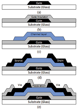
Fig. 1: Fabrication steps for TOS TFTs include (a) gate definition by lift-off, (b) gate-insulator deposition by RF magnetron sputtering, (c) channel layer deposition and definition by RF magnetron sputtering, (d) source/drain (S/D) definition by lift-off, and (e) passivation by RF magnetron sputtering.
The bonding structure in the amorphous oxide semiconductor, e.g., a-InGaZnO (IGZO), is very different from that of conventional semiconductors such as a-Si and LTPS. In the oxide semiconductor, the atomic structure for conduction-band minima (Em) is based on ionic bonding.18 This implies that the connection between neighboring atoms is insensitive to variations in bonding angle, leading to high-quality film even in the amorphous phase. That is the main reason why this class of semiconductors provides higher mobility compared to a-Si. Figure 2(a) illustrates the orbital picture of Em in oxide semiconductors in both crystalline and amorphous phases. As can be seen, there is a conduction path despite variations in bond angle. In contrast, the conduction band in silicon is based on hybrid orbitals (sp3) with strong sensitivity to bonding angle variation, as shown in Fig. 2(b). Therefore, silicon in amorphous phase is less conductive, providing a much lower mobility compared to the oxide semiconductor counterpart. One of the issues
in multi-component oxides (e.g., In-Ga-ZnO) is the compositional disorder arising from a random distribution of metal atoms, e.g., Ga and Zn.18 This leads to conduction-band fluctuations, giving rise to potential barriers above the conduction-band minima (Em).19 Consequently, we have percolation conduction in addition to the conventional trap-limited conduction.20 More importantly, because the oxide semiconductor has a large Bohr radius, this class of the material has a wide band gap (~3 eV) and thus high-optical transparency (~80%).9,21
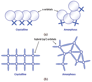
Fig. 2: Above are schematic illustrations of orbitals composed of conduction-band minima (Em) in (a) oxide semiconductor (ionic bonding) and (b) silicon (covalent bonding) in crystalline and amorphous phases.
.
However, the oxide semiconductor has a disadvantage. The presence of oxygen vacancies (V0) located in the gap states near the valence band, as shown in Fig. 3(a), can play the role of absorption sites for visible light. The resulting ionized V0 is located in the vicinity of Em and yields a highly conductive film upon illumination.22 The problem is that the ionized V0 has an outward relaxation with higher energy than the previous state V0, as described in Figs. 3(b) and 3(c).22 So, the ionized condition is maintained even after removal of the light source, suggesting persistence in photoconductivity (PPC), resulting in slow recovery. The same is also observed with threshold voltage shift (ΔVT), as discussed in the next section.
(a) 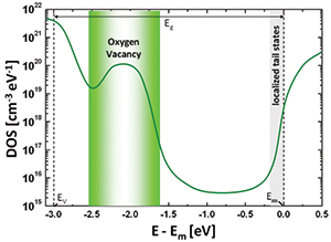
(b) 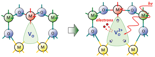 (c)
(c)
Fig. 3: (a) Typical density of states as a function of energy from the conduction band edge (Em) of AOS TFTs indicate oxygen vacancy (V0) sites in the middle of the gap (EV) denotes valence band edge. Schematic bonding structures of the AOS semiconductor show (a) V0 and (b) the ionized V0 (V2+0) under illumination, respectively. Here, V2+0 can release two electrons, having an outward relaxation, suggesting a higher energy compared to the previous state (V0). Here, M denotes the metal atom, e.g., Ga and Zn, and O the oxygen atom.
Optically Induced Instability
The source of the PPC and threshold-voltage shift (ΔVT) under illumination are believed to be the same. Figure 4 compares the transfer characteristics of TFTs after 3 hours of light stress combined with positive/negative bias stress. The spectrum of the light source used is shown in the inset of Fig. 4(a). The optical power is ~40 mW/cm2, while the gate-bias values were 20, 0, and -20 V. As shown in Fig. 4(a), the transfer characteristics show a negative VT shift regardless of bias polarity. This implies that the effect of the ionized oxygen vacancies is dominant and can be explained and described by
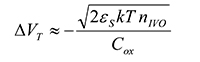
(1)
where εS is the permittivity of the channel layer, kT is the thermal energy, and nIVO is the density of the ionized oxygen vacancies. Charge trapping in the gate dielectric was found to be insignificant.
The PPC is gate-bias dependent, as shown in Fig. 4(b). Here, a negative VGS pulse slows the recombination of PPC by separating the photo-generated e-h pairs. In contrast, a positive VGS pulse accelerates the recovery, which is observed upon release of, and not during, the positive bias pulse. Therefore, a positive gate pulse enables an operational scheme for managing instability associated with PPC, accelerating recombination of ionization oxygen vacancies.21
(a) 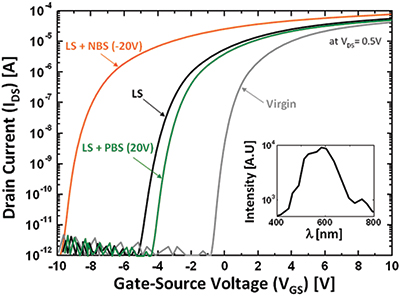
(b) 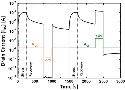
Fig. 4: (a): Shown above are transfer characteristics of IZO/IGZO TFTs subject to 3 hours of light-bias stress of different magnitude and polarity.23 Inset: illumination source spectrum on a semi-log scale. (b) Drain-source current as a function of time subjected to illumination at intensities ~40 and 5 mW/cm2 and recovery under different gate-bias conditions. The dashed lines trace the evolution of bias and light conditions with time. Here, negative VGS slows recovery of PPC while a positive VGS accelerates it.24,25 [(Graphs adapted from K. Ghaffarzadeh et al., SID Symposium Digest of Technical Papers 42, 1154-1157 (2011).]
Applications
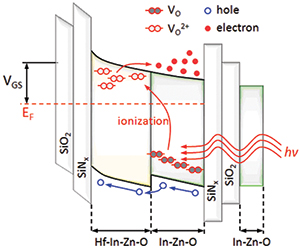
Besides its obvious application in active-matrix displays, the TOS TFT technology, as mentioned earlier, can also be used as photosensors for visible-light applications because of the presence of oxygen vacancies in the sub-gap states.21 For photosensor applications, we need to overcome the slow recovery due to PPC.24 But techniques for adjusting the virgin VT in a dual-gate photo-TFT through independent control of the gates has been reported based on a positive-gate-voltage control scheme.21,24 In the example shown here, the TFT considered is a photosensor for imaging applications, in which a transparent conducting In-rich IZO layer is employed as the top gate as shown in Figs. 5(a) and 5(b) to yield minimum degradation in device photosensitivity. The huge responsivity of the photo-TFT observed [Fig. 5(c)] was attributed to high photoconductive gain
(Gph)24-26 because of efficient e-h separation by virtue of band structure [Fig. 6(b)]. This retards the recombination rate, thus allowing for a longer carrier lifetime (τn). The gain can be represented as follows26:
Gph = τn/τt (2)
Here, τt is the carrier transit time from source to drain, which is independent on τn. The extended τn can be explained using the following equation26:
τn = nIVO/γn2i (3)
where γ is the recombination rate and ni is the intrinsic carrier density. Using this high optical sensitivity, visible-light sensing can be embedded into display panels for interactive applications21,24,25 (see Fig. 6).
(a) 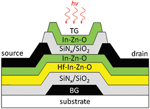
(b)
(c) 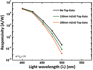
Fig. 5: A schematic diagram of dual-gate photo-TFT is shown in (a); a band diagram upon exposure to light in (b); and responsivity as a function of wavelength for photo-TFT as a function of thickness of top In-rich InZnO gate in (c).
(a) 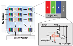
(b)
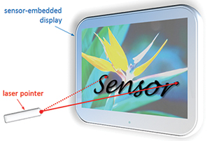
Fig. 6: Shown in (a) is a typical architecture of an image sensor embedded in an active-matrix display with the pixel structure.24,25 Below, (b) indicates the desired display with the word “sensor” written by a laser pointer.24,25
Looking Ahead
The oxide materials system can be judiciously tailored for display applications that also embed photosensor arrays based on the TFT architecture to enable fast recovery times overcoming issues related to persistent photoconductivity. The results demonstrated here signify the feasibility of transparent interactive active-matrix displays with embedded imaging that enable both touch and touch-free operation.
References
1R. Chaji and A. Nathan, Thin Film Transistor Circuits and Systems (Cambridge University Press, Cambridge, 2013).
2Corning’s A Day Made of Glass, Corning (http://www.corning.com), New York (2011).
3J. F. Wager, Science 300, No. 5623, 1245–1246 (23 May 2003).
4N. Neves, R. Barros, E. Antunes, J. Calado, E. Fortunato, R. Martins, and Isabel Ferreira, J. European Ceramic Society 32, No. 16, 4381–4391 (Dec. 2012).
5J. F. Wager, D. A. Keszler, and R. E. Presley, Transparent Electronics (Springer, New York, 2008).
6Smart Windows Markets 2012, NanoMarkets, LC (Feb. 2012).
7K. Nomura, T. Kamiya, H. Ohta, K. Ueda, M. Hirano, and H. Hosono, Appl. Phys. Lett. 85, 1993 (2004).
8R. Martins, A. Nathan, R. Barros, L. Pereira, P. Barquinha, N. Correia, R. Costa, A. Ahnood, I. Ferreira, and E. Fortunato, Advanced Materials 23, No. 39, 4491–4496 (Oct. 18, 2011).
9R. L. Hoffman, B. J. Norris, and J. F. Wager, Appl. Phys. Lett. 82, 733 (2003).
10J. Robertson, J. Non-Crystalline Solids 358, 2437 (2012).
11R. A. Street, Hydrogenated Amorphous Silicon (Cambridge University Press, 2005).
12J. I. Song, J. S. Park, H. Kim, Y. W. Heo, J. H. Lee, J. J. Kim, G. M. Kim, and B. D. Choi, Appl. Phys. Lett. 90, 022106-1-3 (Jan 2007).
13F. M. Hossain, J. Nishii, S. Takagi, A. Ohtomo, T. Fukumura, H. Fujioka, H. Ohno, H. Koinuma, and M. Kawasaki, J. Appl. Phys. 94, 7768–7777 (Dec 2003).
14K. Nomura, H. Ohta, A. Takagi, T. Kamiya, M. Hirano, and H. Hosono, Nature 432, 488–492 (Nov 2004).
15S. Jeon, S. I. Kim, S. Park, I. Song, J. Park, S. Kim, and C. Kim, IEEE Elect. Dev. Lett. 31, No. 10 (2010).
16M. Ofuji, K. Abe, H. Shimizu, N. Kaji, R. Hayashi, M. Sano, H. Kumomi, K. Nomura, T. Kamiya, and H. Hosono, IEEE Elect. Dev. Lett. 28, 273-5 (2007).
17H. Hosono et. al., J. Non-Crystalline Solids 352, 851-858 (Jun 2006).
18A. Takagi, K. Nomura, H. Ohtab, H. Yanagia, T. Kamiya, M. Hirano, and H. Hosono, Thin Solid Films 486, 38–41 (2005).
19V. I. Arkhipov, E. V. Emelianova, and G. J. Adriaenssens, J. Phys.: Condens. Matter. 12, 2021–2029 (2000).
20S. Lee, K. Ghaffarzadeh, A. Nathan, J. Robertson, S. Jeon, C. Kim, I. H. Song, and U. I. Chung, Appl. Phys Lett. 98, 203508 (2011).
21S. Jeon, S.-E. Ahn, I. Song, Y. Jeon, Y. Kim, S. Kim, H. Choi, H. Kim, E. Lee, S. Lee, A. Nathan, J. Robertson, C. J. Kim, U-I. Chung, I. Yoo, and K. Kim, IEEE IEDM Technical Digest, 14.3.1–14.3.4 (2011).
22A. Janotti and C. G. Van de Walle, Appl. Phys. Lett. 87, 122102 (2005).
23T. Kamiya and H. Hosono, Intl. J. Appl. Ceram. Technol. 2, 285 (2005).
24S. Jeon, S.-E. Ahn, I. Song, C. J. Kim, U-I. Chung, E. Lee, I. Yoo, A. Nathan, S. Lee, J. Robertson, and K. Kim, Nature Materials, 11, (Feb. 2012).
25S.-E. Ahn, I. Song, S. Jeon, Y. W. Jeon, Y. Kim, C. J. Kim, B. Ryu, J.-H. Lee, A. Nathan, S. Lee, G. T. Kim, and U-I.
Chung, Advanced Materials 24, No.19 (May 2012).
26S. Lee, J. Robertson, and A. Nathan, “How to Achieve Ultra High Photoconductive Gain for Transparent Oxide
Semiconductor Image Sensors,” IEEE IEDM Technical Digest (2012). •
Arokia Nathan is with the Department of Engineering, University of Cambridge, UK. He can be reached at an299@cam.ac.uk. Sungsik Lee is with the London Center for Nanotechnology, University College London, UK. Sanghun Jeon, Ihun Song, and U-In Chung are with the Semiconductor Device Laboratory, Samsung Advanced Institute of Technology, Korea.