Flexible AMOLED Displays Make Progress
Flexible AMOLED Displays Make Progress
AMOLED technology is an emerging technology that has gained tremendous attention in part because of its potential for flexibility. This article provides an overview of AUO’s progress in AMOLED technology, from fixed curve to bendable, and now moving toward a foldable display.
by Annie Tzuyu Huang, Chi-Shun Chan, Cheng-liang Wang, Chia-Chun Chang, Yen-Huei Lai, Chia-Hsun Tu, and Meng-Ting Lee
ACTIVE-MATRIX light-emitting diodes (AMOLEDs) are a crucially important and ongoing display research subject for many reasons. They enable, to varying degrees, displays with a slim form factor, fast switching times (~µsec), energy efficiency, wide color gamut, deep blacks and high contrast, and last, but not least, flexibility, especially compared to that of LCDs. Because LCDs utilize a backlight and require a fixed cell-gap distance, it is difficult for LCDs to achieve flexibility. Because of the recent advances made in both thin-film encapsulation and the thermal resistance of plastic film (see below), we are now moving toward the goal of a truly flexible AMOLED display. In this article, several important technology developments related to AUO’s recent work with flexible AMOLED displays will be discussed.
Material Concerns
Encapsulation methods and materials are crucial for AMOLED displays because AMOLEDs degrade rapidly in the presence of oxygen and moisture. Conventional glass-based AMOLED displays use glass encapsulation with frit sealing around the perimeter of the display to prevent moisture and oxygen from
entering the OLED panel.1 In general, this encapsulation needs to achieve a water-vapor transmission rate (WVTR) of ~10-6 g/m2/day for an AMOLED device to pass its reliability tests, which guarantees 5 years of lifetime. An AMOLED display with glass encapsulation is generally as thick as 7 mm [as shown in Fig. 1(a)]. Even though a thinner panel could be achieved with additional glass-thinning processes after assembly, the panel would not be flexible, similar to an LCD panel. If glass encapsulation can be eliminated, AMOLED displays gains the advantage of significant flexibility.
Creating Stacks for Flexible AMOLED Structures
Creating a flexible OLED display imposes several additional challenges, including proper backplane selection and elimination of the glass layers, which, in turn, re-introduces the problem of environmental contamination. Special steps must be taken in order to create a flexible-display stack that is also able to achieve sufficient barrier protection. In general, the core of a flexible AMOLED display has the structure shown in Fig. 1(b), where a top-emission AMOLED display is composed of a substrate with a TFT array deposited with OLED layers and thin-film encapsulation (TFE) on the top. Currently, LTPS-TFT is the most common TFT backplane, due to its higher mobility and better electrical performance compared to other technologies such as amorphous silicon or IGZO.2 A circular polarizer is then laminated above the TFE layer and the bottom of the substrate is laminated with a supporting back film. As mentioned earlier, the function of the TFE layer is to protect the AMOLED device from the interaction of oxygen and moisture and obtain the WVTR property of 10-6 g/m2/day. Without an additional moisture- and oxygen-blocking layer, none of the plastic layers alone is enough to protect the AMOLED materials properly. Therefore, it is critical to develop a TFE layer structure that can achieve the WVTR requirement.
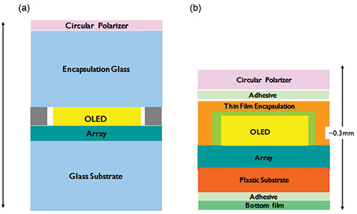
Fig. 1: The structure of a conventional glass-based AMOLED display is shown in (a). The structure of a current flexible AMOLED display (not drawn to scale) appears in (b).
One of the best-known approaches thus far is to form multiple layers of organic and inorganic thin films, the so-called Vitex technology (after Vitex Systems,
the company that developed it).3–5 Several authors have reported that flexible encapsulation layers made of alternating Al2O3 and polyacrylate layers can achieve 10-6 g/m2/day. The inorganic layers act as the primary moisture barrier while the organic layers decouple the pinholes of the inorganic layers. As a result, the diffusion length for water to permeate through the stack is extended. In addition, the organic layer works as a planarization layer that provides a smoother surface for the deposition of the following inorganic layer and eases the lamination process applied after the TFE structure is complete. With an alternative stacking approach similar to that shown in Fig. 2 (compared to a single inorganic layer), this type of structure reduced the WVTR
dramatically, from 10-3 to 10-4 or 10-6 g/m2/day.
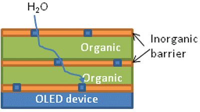
Fig. 2: Inorganic and organic layers are stacked alternately in a thin-film-encapsulation stack that greatly reduces water-vapor transmission rates.
Alternative Approaches to Thin-Film Encapsulation
This Vitex structure is effective, but the fabrication process has proven complicated and costly, and research into lower cost and simpler process TFE has been ongoing. One example is the deposition of hexamethyl-disiloxane (HMDSO). Recently, HMDSO has become an attractive material for TFE because it can possess
either inorganic or organic properties through simple process tuning using a plasma-enhanced chemical-vapor deposition (PECVD) process.6–8 Increasing or decreasing the O2 content during deposition will cause the film to be more inorganic- or organic-like, respectively.
It is important to consider the optical properties as well as the moisture-blocking abilities of TFE structures, and, accordingly, AUO has recently developed a hybrid structure using HMDSO as a precursor and an optical enhancement layer as shown in Fig. 3. With the application of optical enhancement layers, the performance of OLED displays with TFE is comparable to glass encapsulation in efficiency and color coordinates as well as viewing-angle properties. More related research is under way, and recent development has shown that this structure is able to pass 500-hour aging at 60°C and 90%RH.
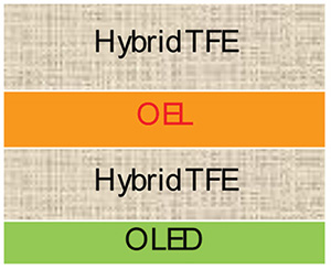
Fig. 3: A recent development from AUO shows a structure incorporating a hybrid TFE with HMDSO as a precursor with optical enhancement layers.
Pros and Cons of Circular Polarizers
Adding a circular polarizer to the top of the stack, as shown in Fig. 1, has advantages and disadvantages. The function of a circular polarizer is to filter out ambient light. Because the top of the OLED region consists of electrodes with high reflection (e.g., Ag) as shown in Fig. 4, at the region without the polarizer, the OLED electrode reflects incident light and the off-state does not appear dark. As a result, contrast ratio suffers. As shown in Fig. 5(a), a circular polarizer consists of a linear polarizer and a 1/4 λ retarder film. A linear polarizer first allows only linearly polarized light passing through. The 1/4 λ retarder film then turns the linear waves to circular waves. When circular rays strike a reflecting surface (e.g., an electrode of a top-emission OLED), their phase relationship is reversed. This results in reflected light that is now in the opposite orientation to the polarizer stack; therefore, the reflected light rays are blocked from leaving the stack. Utilization of a circular polarizer therefore reduces internal reflections and increases the contrast ratio of the display. However, the drawback is that the luminance of the unpolarized light emitted from the AMOLED stack is also reduced by as much as 60%, requiring higher power consumption to achieve the desired luminance levels of the display.
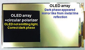
Fig. 4: An OLED panel is shown at left with a circular polarizer and, at right, without one.
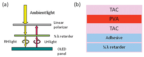
Fig. 5: The basic components of a circular polarizer is shown in (a). For a combination of a linear polarizer and a 1/4 λ retarder, all ambient light is absorbed. A typical layered structure for a circular polarizer is shown in (b).
Fixed Curved to Bendable
In 2013, AUO demonstrated a fixed-curve AMOLED panel at Touch Taiwan (International Smart Display and Touch Panel Exhibition) as shown in Fig. 6. The AMOLED display used side-by-side RGB stripe technology with a fine-metal mask to successfully produce a 257-ppi mobile display. The 4.3-in. flexible display incorporated flexible materials and thin-film-encapsulation technology. This display was only 0.2 mm thick and could be formed into a curved shape with a radius smaller than 60 mm. At both Touch Taiwan 2014 and Display Week 2014, AUO showcased a 5-in. flexible AMOLED display using AUO subpixel-rendering technology with an on-cell touch panel on a plastic substrate using TFE technology. This stack allowed a minimum bending radius to less than 10 mm. The panel was also 0.2 mm thick and could be used for smartphones with screens extended to the sides. Users could thus set function keys at desired locations to increase more space for operation and viewing area. To obtain a bent edge, curve lamination was utilized.
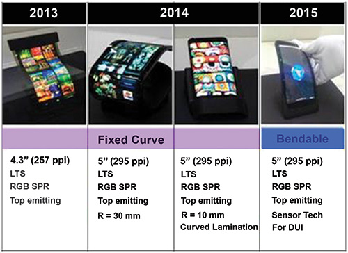
Fig. 6: The above photos of flexible AMOLED displays from AUO range from a 4.3-in. fixed curve in 2013 to a 5-in. bendable model in 2015.
AUO then demonstrated a 5-in. 295-ppi bendable AMOLED prototype with a bending sensor at Touch Taiwan 2015 and IWFP (International Workshop on Flexible and Printable
Electronics) Korea, as shown in Fig. 6. This flexible AMOLED display incorporates a novel bending interactive interface that works differently from a flat-panel display. It allows users to bend the panel and manipulate the size and direction of the
display’s active area. The content display on the screen can be manipulated by twisting and bending the unit. The fundamental concept of this technology is to input commands through changing the geometric profile of the display rather than through touch sensing. In other words, the display receives information as it is bent, rolled, twisted, or folded by the user. The geometric information of the display can be derived from the measurement of the mechanical strain. The relationship of the measured resistance ΔR and mechanical strain ε in a strain sensor can be expressed as the following equation:
ΔR/R = F · ε,
where R is the initial resistance of the strain gauge when no strain is applied and F is the gauge factor, a constant coefficient depending on the gauge property. The curvature κ along the strain direction is proportional to the measured strain as
κ = ε/y
where y is the distance between the layer of strain gauge and the neutral plane of the flexible display. As shown in Fig. 7, this prototype comprises a 5-in. flexible display with a film-type strain gauge laminated on the back. With precise calibration, we can obtain accurate information of the six bending modes as shown in Fig. 8 from the resistance change measured from the strain gauge of the bending sensor.
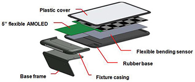
Fig. 7: The structure design of a bendable phone prototype includes both a bending sensor and a touch sensor.
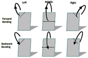
Fig. 8: Six modes of bending operations for a bendable phone are shown.
Bendability Enables a New Interface
Navigating Google Earth is one possible use for this technology. Bending left or right in forward or backward direction rotates the earth, while bending forward or backward at the middle can zoom in and zoom out the earth, respectively. This bendable phone technology with a flexible AMOLED display provides more intuitive operation and control that bring the user experience to the next level. (For more about this functionality, see the article, “A Flexible Display Enables a New Intuitive User Interface,” in the February 2011 issue of ID, which discusses research by Toshiba. The difference between the authors’ work and Toshiba’s is that the former puts multiple sensors on films so that strain can be detected at multiple bending angles.)
Moving toward Foldable Displays
A structure utilizing a polarizer does eliminate the reflectivity of ambient
light. However, as mentioned previously, the existence of the polarizer also increases power consumption because the polarizer unavoidably absorbs at least half of the light emitted by the display. As shown in Fig. 5(b), a circular polarizer consists of a multilayered structure with a linear polarizer and a 1/4 λ retarder film. Polarizing properties are usually obtained by straining polyvinyl alcohol (PVA) and fixing this material by laminating it between TAC films. Therefore, it has poor mechanical properties in comparison to alternative polymer films,
such as polyethylene terephthalate (PET). Additionally, when this kind of polarizer undergoes environmental reliability tests such as high-temperature storage, it tends to deform as shown in Fig. 9. A coating-type polarizer is a possible alternative, but this type of polarizer has not been mass produced.
Fig. 9: A polarizer deforms after a reliability test.
Replacing Polarizers with Color Filters
A potential solution to achieve high contrast without as much loss of display luminance is to utilize a color-filter layer instead of a polarizer. As shown in Fig. 10, such a structure consists of a touch sensor and a color filter at the top. The assembly is completed with a moisture barrier. Without the use of a polarizer, the flexible properties of the display are not constrained by the thickness of the polarizer. The thickness of the top and bottom films can be adjusted to obtain a symmetric panel stacking structure (SPS) with the TFT/OLED/TFE located at the neutral plane of the entire structure instead of at the polarizer layer in the original asymmetric panel structure (APS), as shown in Fig. 11.
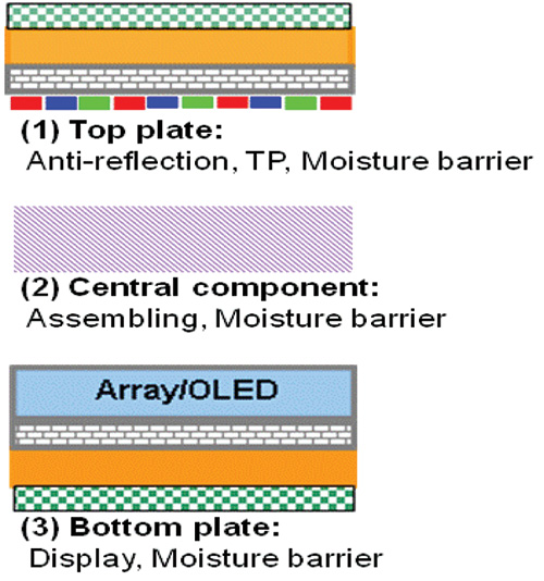
Fig. 10: The layers of an SPS (symmetric panel stacking structure) consist of a top plate and color-filter layer, assembled with an OLED array using a moisture barrier.
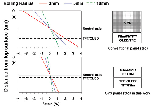
Fig. 11: Strain is shown for different film layers at different rolling radii in (a), an APS structure, and (b) an SPS structure.
The color filter utilized was fabricated on a transparent flexible substrate. The black matrix was first deposited, followed by a single color-filter layer with red, blue, and green color coated side by side. The flexible substrate was further laminated with a top film for additional support and to meet optical requirements.
As mentioned earlier, when plastic material such as PET instead of a complex multi-layered polarizer is utilized, the mechanical property of the flexible AMOLED device is greatly improved in terms of bearing more strain and demonstrating less stiffness. The total thickness can be also reduced to one third of the APS structure, as shown in Table 1. With the application of a color filter, as shown in Fig. 12(a), when the ambient light first enters the color filter, for example, only red light is able to pass through the red color filter and hits the red OLED layer and is reflected back to the ambient through the red color filter again. As a result, at on-state, the emitted light from the display shows both the red light emitted from the OLED panel plus the red reflected ambient light, not the other colors. Fig. 12(b) shows the reflectivity of the SPS structure and the APS structure. Most importantly, as shown in Fig. 13, using the same 5-in. panel, the SPS structure can reduce power consumption by half and double the lifetime.
Table. 1: A comparison of total thickness and stiffness is shown for SPS at left and APS at right.
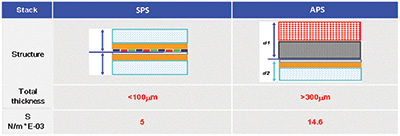
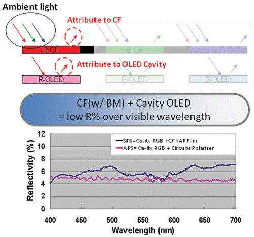
Fig. 12: The path of ambient light into an SPS structure appears at top. At bottom is a comparison of reflectivity for SPS and APS structures.
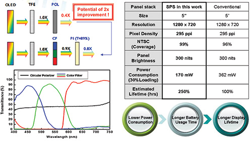
Fig. 13: A comparison of power consumption and light absorption for SPS and APS (conventional) structures shows that the SPS stack consumes less power.
Recipe for a Foldable Display
With the much improved mechanical properties of SPS as compared to APS, we have obtained a potential candidate for foldable displays. As shown in Fig. 14, a 5-in. panel with an SPS structure was prepared and folded repeatedly at the center. More than 500K folding cycles at a bending radius of 4 mm showed no damage on TFT/OLED/TFE and no effect on the panel’s optical property.
Flexible AMOLED displays have come a long way from fixed curve to foldable, but more effort is necessary (and currently under way) to realize the latter in terms of taking demo samples from a lab setting to mass production. With continuous effort in materials research, structural improvements, and additional innovative ideas, it is likely that we are steadily moving toward a bright future with flexible AMOLED technology.
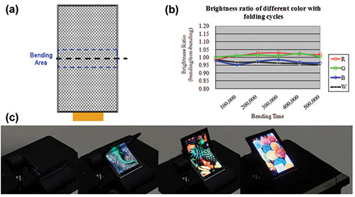
Fig. 14: The bending region of an SPS 5-in. foldable OLED display is shown in (a). In (b), the brightness ratio between bending and non-bending regions is compared after 50K bending cycles. Photos depicting the bending sequence of the 5-in. foldable AMOLED display appear in (c).
References
1J. S. Lewis and M. S. Weaver, “Thin-Film Permeation-Barrier Technology for Flexible Organic Light-Emitting Devices,” IEEE J. Selected Topics in Quantum Electronics 10, 45 (2004).
2J. F. Wager, “Flat-Panel-Display Backplanes: LTPS or IGZO for AMLCDs or AMOLED Displays,” Information Display 30, No. 2, 26–29 (Mar/April 2014).
3A. B. Chwang, “Thin-film-encapsulated flexible organic electroluminescent displays,” Appl. Phys. Lett. 83(1), 413–415 (2003).
4M. S. Weaver, L. A. Michalski, K. Rajan, M. A. Rothman, J. A. Silvernail, J. J. Brown, P. E. Burrows, G. L. Graff, M. E. Gross, P. M. Martin, M. Hall, E. Mast, C. Bonham, W. Bennett, and M. Zumhoff, “A single-layer permeation barrier for organic light-emitting displays,” Appl. Phys. Lett. 81, 2929 (2002).
5C. S. Suen and X. Chu, “Multi thin-film barrier protection of flex-electronics,” Solid State Technology 51, 36–39 (2009).
6C-H. Su and T-C. Wei, “Display Device with Passivation Structure,” U.S. Patent No. 7030557 B2 (2006).
7P. Mandlik, J. Gartside, L. Han, I. C. Cheng, S. Wagner, J. A. Silvernail, R. Q. Ma, M. Hack, and J. J. Brown, “A single-layer permeation barrier for organic light-emitting displays,” Appl. Phys. Lett. 92, 10, 103309 (2008).
8L. Han, P. Mandlik, J. Gartside, S. Wagner, J. A. Silvernail, R. Q. Ma, M. Hack, and J. J. Brown, “Properties of a permeation barrier material deposited from hexamethyl disiloxane and oxygen,” J. Electrochem. Soc. 156, No. 2, H106–H114 (2009). •
Annie T. Huang and Chi-Shun Chan are senior research engineers, Cheng-Liang Wang, Yen-Huei Lai, and Chia-Hsun Tu are managers, Chia-Chun Chang is a user interface designer of flexible sensors, Yen-Huei and Meng-Ting Lee are currently senior managers, all at AUO. M-T. Lee can be reached at mt.lee@auo.com.