High-Performance White-OLED Devices for Next-Generation Solid-State Lighting
High-Performance White-OLED Devices for Next-Generation Solid-State Lighting
The efficacy of white OLEDs has reached 100 lm/W with RGB-phosphorescent emitters and light-extraction technologies. OLEDs have therefore already exceeded the efficacy of typical lighting equipment with fluorescent lamps.
by Kazuyuki Yamae, Hiroya Tsuji, Varutt Kittichungchit, Nobuhiro Ide, and Takuya Komoda
LIGHTING represents almost 20% of global electricity consumption. A savings potential of more than 1000 TWh (terawatt hours) per year by 2030 is possible if conventional inefficient lamps are replaced by highly efficient solid-state lighting (SSL).1,2 The total electricity consumption of the world was approximately 18,000 TWh in 2010, according to Japan’s Agency of Natural Resources and Energy (www.enecho.meti.go.jp/english/). Light-emitting diodes (LEDs) are a well-known source of highly efficient solid-state lighting (SSL), and LED equipment has gradually been replacing conventional lighting such as that based on incandescent bulbs. Organic light-emitting diodes (OLEDs) are another candidate for next-generation SSL because they are compact, lightweight, highly responsive, and highly flexible in terms of design. Commericalized OLEDs have already exceeded the efficiency of incandescent bulbs. However, they have not yet surpassed LEDs.
The efficiency of OLEDs is mainly determined by three factors: internal quantum efficiency (IQE), electrical efficiency (EE), and light-extraction efficiency (LEE). First, optimization of the carrier balance with energy levels and the mobility of stacked layers for emission, transportation, injection, or blockage is required to maximize IQE, especially for effective radiative hole–electron recombination. According to spin statistics, the hole–electron recombination yields singlet and triplet excitons by a ratio of 1:3, respectively. It is well known that phosphorescent OLEDs enable radiation from triplets and that its IQE has already reached nearly 100%.3,4
EE is inversely proportional to the driving voltage, which is controlled by charge injection and carrier transfer. High-mobility materials or electrical doping techniques have enabled an extremely low driving voltage of OLED devices that has come close to theoretical limits.5 However, restrictions are required to achieve both low driving voltage and a long lifetime because of the fundamental issue of durability in organic materials. These architectures can also suffer from resistive losses induced by the relatively large currents required by low driving voltages.
The largest potential of the aforementioned three factors is in LEE. Only about 20% of the total generated light can escape to the air from conventional OLED devices, due to total internal reflection (TIR) at the interfaces as shown in Fig. 1 and explained by Snell’s law as one of the limiting factors in LEE. Since organic layers and glass substrates have higher refractive indices than air, light that reaches the outer boundaries of the device at wide incident angles encounters total internal reflection (TIR) and is trapped inside the device instead of being able to escape. The reflected light is then absorbed back into the organic layers or electrodes.
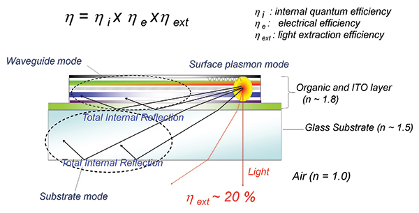
Fig. 1: A standard light-extraction model for OLED shows total internal reflection (TIR) at two interfaces.
Various optical structures with micro-sized texture or nano-sized gratings fabricated on the surface of the substrate are simple methods that can be used
to improve LEE.6 However, these technologies are not able to extract the remaining light confined in the transparent electrode and organic layers – this trapped light is called the waveguide mode.
Some internal light out-coupling structures such as scattering layers or diffraction gratings fabricated in the organic layers have been useful in reducing the waveguide mode and have achieved better LEE.7-9 However, those scattering layers or gratings usually have rough surfaces, which reduce reliability through current leakage or short circuits. A special high refractive index (n ~ 1.8) substrate with micro-patterned texture has achieved excellent LEE because of the improved transmission from thin layers to the substrate.10 However, reliable high-refractive-index glass (n ~ 1.8) at low cost is not commercially available for large-area substrates applicable to OLEDs.
In this article, we focus on the progress of light-extraction technology using a Built-up Light Extraction Substrate (BLES)11,12 – a technology developed by Panasonic engineering. Using this BLES, an efficacy of over 100 lm/W was achieved in combination with developed white-phosphorescent OLED devices. This measure of 100 lm/W is widely recognized as the first destination for next-generation lighting because the efficacy exceeds current typical lighting applications using fluorescent lamps.
Built-Up Light-extraction Substrate (BLES)
A cross section of a BLES structure with a bottom-emitting OLED is shown in Fig. 2. BLES comprises a transparent electrode, a high-refractive-index (n = 1.77 at 550 nm) micro-lens-array (MLA) structure made from polyethylene naphthalate (PEN) film, and a glass substrate for encapsulation. An air gap exists between the MLA and the glass substrate.
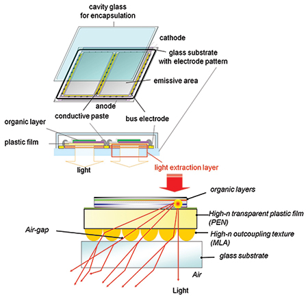
Fig. 2: This cross section of an OLED shows the structure of the built-up light-extraction substrate (BLES).
The BLES was fabricated as follows: A transparent electrode was previously deposited on one surface of PEN film. MLA was fabricated onto the opposite side of the film. This film was then laminated to a glass substrate with the MLA side facing the glass. The micro-patterned texture of the MLA was attached to the glass substrate, and the air gap naturally occurred between the textures and the glass. This assembly was then vacuum-dried at 80°C for at least 15 minutes in order to remove the residual water and gases before use. After the deposition of the OLED device onto the film on the top side, electrodes on the film were connected to the bus electrodes on the glass substrate with a conductive paste. The film and deposited organic device were completely encapsulated by a cavity glass.
Due to the high-refractive-index structure, light emitted from the organic layers propagates into the PEN and MLA layers without TIR. Owing to the existence of the air gap between the out-coupling texture and glass substrate, extracted light from the MLA was able to transmit into the glass substrate without TIR, and an excellent LEE was expected.
BLES has other merits in addition to the enhancement of light-extraction efficiency. First, the smooth surface of the film is applicable to a large-area OLED device. Second, the rigid protection from water vapor, reactive gases, or other physical damages by the glass substrate enables better durability of the OLED device on the film and micro-textures. Plus, the substrate is appropriate for commercial use because each component is relatively inexpensive compared to high-refractive-index glass.
Optical Design for BLES
The propagating light in BLES is divided into transmitted diffraction and reflected diffraction at the interface of the MLA and the air gap. Transmitted diffraction is extracted from the air without TIR at the glass surfaces as described previously. Reflected diffraction is extracted through the multiple reflections in OLED and BLES, or absorbed. Thus, BLES has the potential to realize excellent LEE while suppressing internal absorption since TIR is almost eliminated. In a conventional structure, the waveguide, substrate, and air modes are 50%, 30%, and 20%, respectively. If we use a high-refractive-index substrate such as PEN, the waveguide mode is transferred to the substrate mode and the substrate and air modes are 80% and 20%, respectively. BLES enables substrate mode to air mode. If we can achieve a no-absorption device, 100% of light is extracted. On the other hand, a conventional structure can achieve only 50%, since the waveguide mode is retained in organic layers and cannot be extracted whether absorption is high or low.
The influence of internal absorption to LEE in BLES was fully investigated to obtain higher LEE. To begin with, the transparency of BLES was examined. The measurement results of reflectance and transmittance of BLES are shown in Fig. 3. To avoid the noise caused by scattering, the MLA was replaced by a flat layer with an equivalent thickness of its height (about 5 µm) as shown in Fig. 3. No absorption was observed in BLES since the summation of reflectance and transmittance was almost 100% in the region of a visible wavelength. Spectral ripples by optical interference were not observed as refractive indices of PEN film and high-n material for MLA was similar.
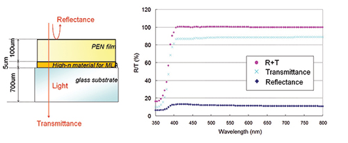
Fig. 3: Reflectance and transmittance measurements for BLES.
On the premise that no-absorption channel is in the BLES, the diffraction at MLA and internal absorption in the OLED became the primary focus of investigation. In this study, the LEE of the OLED with a high-refractive-index extraction layer was simulated by a calculation model combined with rigorous coupled wave analysis (RCWA) and ray-tracing.13 The calculated model is shown in Fig. 4. Model A was almost equivalent to BLES, which was composed of a high-refractive-index substrate (n = 1.78) and MLA (n = 1.78). The glass substrate under the MLA was removed to simplify the calculation because its absorption and influence on LEE did not need to be taken into consideration in this case. Model B was a conventional light- extraction structure composed of typical external out-coupling MLA film (n = 1.52) that had the same texture as Model A with a glass substrate (n = 1.52).
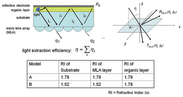
Fig. 4: Two different optical simulation models (A and B) were used for BLES.
The simulation algorithm is described as follows. First, the incident light I1(θi,φi) can be calculated by using a Fresnel coefficient in the OLED multilayers. θi and φi are the incident and azimuthal angles, respectively. The average value of p and s polarizations is applied to simplify the calculation. The total radiation for the first incidence is expressed by
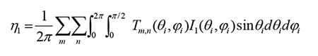 (1)
(1)
The integral numbers of m,n are diffraction orders of the x and y directions. Tm,n(θi,φi) is the transmittance for (m,n) calculated by using RCWA. On the other hand, the reflection for each direction at the first incidence can
be given by a function of the reflection angles (θr,φr) as
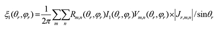 (2)
(2)
Rm,n(θr,φr) is the reflectance for (m,n) calculated by using RCWA. Vm,n is a rewrite of sinθi as a function of θr,φr, and |Jr,m,n| is the Jacobian determinant ς(θr,φr)/ς(θr,φr. The second incidence is obtained from the reflectance Ro(θr,φr), which is calculated by using the Fresnel coefficient matrix for the OLED multilayers and ξ1(θr,φr), which is calculated by using Eq. (2). θr,φr are regarded as the second incident angles because the incident angle of light is not converted at the reflective electrode:
I2(θr,φr) = Ro(θr,φr)ξ1(θr,φr) (3)
Therefore, the radiation for the second incidence η2 is determined by substituting Eq. (3) into Eq. (1). The radiation of each incidence for the multiple reflection of light can be determined in the same manner because its angle is not converted in the OLED and electrodes. Consequently, the extraction efficiency η is described as the sum of all radiation from the micro-structure:
 (4)
(4)
The calculated result is shown in Fig. 5. It is indicated that the influence of internal absorption was more dominant in Model A with its high-refractive-index substrate than in Model B with its low-refractive-index substrate. The high-refractive-index substrate removed the waveguide mode, which was confined within the organic layers. Thus, all light from the emitting layer could pass through the optical pass with multiple reflections as described. Therefore, the LEE was more strongly influenced by the internal absorption in the OLED with a higher-refractive-index substrate.
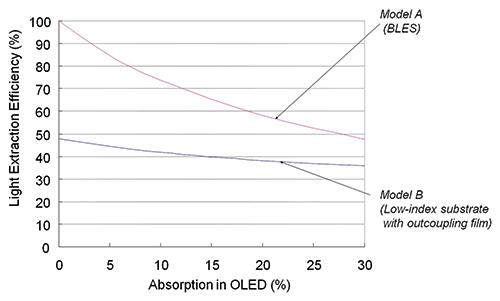
Fig. 5: The optical simulation result of LEE for both Models A and B.
Then, the high-absorption layers were carefully specified and replaced by lower-absorption materials. A comparison of light-extraction structures (BLES and conventional outcoupling film) with different absorption devices is shown in Fig. 6. The optical enhancement of the external quantum efficiency (EQE), which is in proportion to LEE, was obviously improved with lower absorption. The trend was more dominant in the BLES than with the the conventional structure with external out-coupling film.
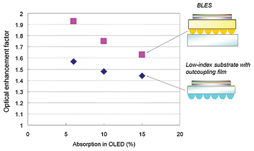
Fig. 6: Optical enhancement with lower absorption was better for BLES than for conventional out-coupling film.
Performance of the Two-Unit Phosphorescent White OLED
The improvement of EE was also studied due to the different driving voltages among devices and because the theoretical energy gap was still large. Typically, the blue-phosphorescent host that enables high quantum efficiency has poor injection and transport properties.14,15 Thus, we assumed that the blue-phosphorescent emitting layer was the main component of high voltage. In this study, the interfacial injection barrier between the electron-transport layer and the blue-phosphorescent emissive layer was examined. Various electron-transport materials with different energy levels were investigated, and the driving voltage was reduced without being a crucial issue to the quantum efficiency and lifetime. Meanwhile, the injection of holes into the blue-phosphorescent emissive layer
was also investigated. The use of the carrier-balancing design resulted in a successful decrease in driving voltage.
The authors developed two-unit all-phosphorescent white-OLED devices that were optimized for maximized IQE and lifetime, minimized driving voltage, and proper
color coordinates. The low-absorption materials, specific light-distribution design, and voltage-reduction technologies as previously mentioned were also applied. The performance of fabricated devices with 1-cm2 pixels is shown in Table 1. The luminance dependence on efficacy at Device A is shown in Fig. 7. Device A showed an extremely high efficacy of 114 lm/W and a quite long half-decay lifetime of over 100,000 hours. It also showed 125 lm/W at 100 cd/m2 and 102 lm/W at 3000 cd/m2. Over 100 lm/W was maintained up to a high luminance of about 4000 cd/m2. LEE was dramatically improved due to the low-absorption materials and specific distribution pattern with BLES. This indicated that almost half of the light was extracted from the emitting layer because an EQE of about 100% was achieved in the two-unit device. The EE was also improved, and the voltage was reduced by about 0.6 V compared to that of Device C.
Table 1: The performance of fabricated all-phosphorescent OLED devices A, B, and C (1-cm2 pixel) is compared.
| All phosphorescent white OLED |
Device A |
Device B |
Device C |
| Low absorption materials |
optimized |
installed |
installed |
| Specific distribution pattern |
optimized |
installed |
— |
| Lower voltage technologies |
optimized |
installed |
— |
| Luminance |
1,000 cd/m2 |
1,000 cd/m2 |
1,000 cd/m2 |
| Efficacy |
114 lm/W |
101 lm/W |
87 lm/W |
| External quantum efficiency (estimated LEE) |
99% (>49%) |
84% (>42%) |
81% (>41%) |
|
| Driving voltage |
5.5 V |
5.9 V |
6.1 V |
| Estimated lifetime (LT50) |
>100,000 h |
>30,000 h |
>100,000 h |
| CRI |
80 |
86 |
82 |
| Color coordinates |
(0.48, 0.43) |
(0.44, 0.44) |
(0.46, 0.42) |
| Color temperatures |
2,550 K |
3,200 K |
2,800 K |
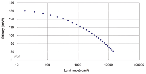
Fig. 7: Luminance depends on efficacy (shown for Device A from Table 1).
Next, a large-area OLED device based on Device A was fabricated. The emission area was 25 cm2. The uniform emission without dark spots and visible defects was realized, as shown in Fig. 8. The properties of this panel are shown in Fig. 9. A quite high efficacy of 110 lm/W and a long lifetime of 100,000 hours at 1000
cd/m2 were also obtained for this OLED panel. The efficacy of the panel decreased by about 3% from the pixel (1 cm2) because the voltage of the panel slightly increased with a voltage drop in the circuit or thermal influence. Color coordinates were in the region of the white color.
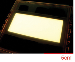
Fig. 8: A large OLED panel (25 cm2) was fabricated based on Device A.
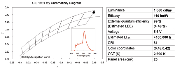
Fig. 9: The performance of the fabricated OLED panel (25 cm2).
Future Prospects for OLED Lighting
Fig. 10 shows the current-efficacy prospects for OLED lighting. The authors’ immediate target in terms of efficacy is 130 lm/W by the end of this year (2013), a target set by the New Energy and Industrial Development Organization(NEDO) at www.nedo.go.jp/english/.
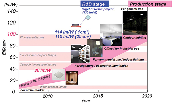
Fig. 10: Current-efficacy prospects for OLED lighting based on the outlook of luminaire efficiency
from Ref. 16.
The arrival of an over 100-lm/W OLED lighting device would be a turning point for entering the general lighting market. It is necessary to develop a light-extraction technology for the waveguide mode such as BLES for the realization of an over 100-lm/W OLED lighting panel. Particular effort should be focused on issues such as reliability, productivity, and cost competitiveness in order for OLED lighting to reach the marketplace for signage, decorative illumination, office and industrial use, and indoor and outdoor lighting. Those development activities are also now ongoing in parallel.
Acknowledgments
This work was supported by NEDO as “Fundamental Technology Development of Next Generation Lighting of High-efficiency and High-Quality” project started in March 2010. We also thank Idemitsu Kosan Co., Ltd., as a member of the project, and also Universal Display Corp. and Nippon Steel & Sumkin Chemical Co., Ltd., for their kind provisions of high-performance materials.
References
1“25 Energy Efficiency Policy Recommendations,” International Energy Agency (2011).
2“Monthly Electricity Statistics,” International Energy Agency (2013).
3C. Adachi, M. A. Baldo, M. E. Thompson, and S. R. Forrest, “Nearly 100 % internal phosphorescence efficiency in an organic light-emitting device,” J. Appl. Phys. 90, 5048 (2001).
4M. A. Baldo, D. F. O’Brien, Y. You, A. Shoustikov, S. Sibley, M. E. Thompson, and S. R. Forrest, “Highly efficient phosphorescent emission from organic electroluminescent devices,” Nature 395, 151 (1998).
5R. Meerheim, K. Walzer, G. He, M. Pfeiffer, and K. Leo, “Highly efficient organic light emitting diodes (OLED) for displays and lighting,” Proc. SPIE 6192, 61920P/1 (2006).
6T. Komoda, H. Tsuji, N. Ito, T. Nishimori, and N. Ide, “High-Quality White OLEDs and Resource Saving Fabrication Processes for Lighting Application,” SID Symposium Digest Tech. Papers, 993 (2010).
7Y. Sun and S. R. Forrest, “Enhanced light out-coupling of organic light-emitting devices using embedded
low-index grids,” Nature Photonics 2, 483 (2008).
8J.-H. Jang, M.-C. Oh, T.-H. Yoon, and J. C. Kim, “Polymer grating imbedded organic light emitting diodes with improved
out-coupling efficiency,” Appl. Phys. Lett. 97, 123302 (2010).
9B.Riedel, J. Hauss, U. Geyer, J. Guetlein, U. Lemmer, and M. Gerken, ”Enhancing outcoupling efficiency of indium-tin-oxide-free organic light-emitting-diodes via nanostructured high index layers,” Appl. Phys. Lett. 96, 243302 (2010).
10S. Reineke, F. Lindner, G. Schwartz, N. Seidler, K. Walzer, B. Lüssem, and K. Leo, “White organic light-emitting diodes with fluorescent tube efficiency,” Nature 459, 234 (2009).
11T. Komoda, K. Yamae, V. Kittichungchit, H. Tsuji, and N. Ide, “Extremely High Performance White OLEDs for Lighting,” SID Symposium Digest Tech. Papers, 610 (2012).
12K. Yamae, H. Tsuji, V. Kittichungchit, Y. Matsuhisa, S. Hayashi, N. Ide, and T. Komoda, “High-Efficiency OLEDs with Built-up Outcoupling Substrate,” SID Symposium Digest Tech. Papers, 694 (2012).
13H. Kikuta, S. Hino, and A. Maruyama, “Estimation method for the light extraction efficiency of light-emitting elements with a rigorous grating diffraction theory,” J. Opt. Soc. Am. A. 23, 1207 (2006).
14N. Chopra, J. Lee, Y. Zheng, S-H Eom, J. Xue, and F. So, “High efficiency blue phosphorescent organic light-emitting device,” Appl. Phys. Lett. 93, 143307 (2008).
15N. Seidler, S. Reineke, K. Walzer, B. Lussem, A. Tomkeviciene, J. V. Grazulevicius, and K. Leo, “Influence of the hole blocking layer on blue phosphorescent organic light-emitting devices using 3,6-di(9-carbazolyl)-9-(2-ethylhexyl)carbazole as host material,” Appl. Phys. Lett. 96, 093304 (2010).
16“Solid-State Lighting Research and Development Multi-Year Program Plan,” U.S. Department of Energy (2013). •
Kazuyuki Yamae, Hiroya Tsuji, Varutt Kittichungchit, Nobuhiro Ide, and Takuya Komoda are with Eco Solutions Company, Panasonic Corp., Japan. K. Yamae can be contacted at yamae.kazuyuki@jp.panasonic.com.