Oxide TFTs for AMOLED TVs
AMOLED TVs using promising oxide semiconductor and thin-film transistors (TFTs) have been unveiled. This article will present the issues, challenges, and concerns of oxide TFTs for AMOLED TVs
byJin-Seong Park
SINCE flexible and transparent amorphous In-Ga-ZnO (indium gallium zinc oxide or IGZO) thin-film transistors (TFTs) were reported in 20041, tremendous progress has taken place with regard to amorphous-oxide semiconductor devices as TFT backplanes. These devices enable high-performance flat-panel displays (FPDs), including active-matrix organic light-emitting-diode displays (AMOLEDs).2 Many FPD manufacturers such as Samsung, LG, Sharp, and AUO have already announced significant investment in large-sized AMOLED panel production based on oxide-semiconductor devices in 2012. Although small-sized AMOLEDs for cell phones using low-temperature polysilicon (LTPS) TFTs are already in large-scale production at Samsung, it is quite significant to hear announcements about adopting oxide-semiconductor devices as backplanes for larger-sized AMOLEDs. According to recent press reports, LG Electronics will sell 55-in. AMOLED TVs to consumers in the first quarter of 2013 (see the CES review in this issue).
For several decades, wide-bandgap oxide materials, including ZnO, Al-doped ZnO, Ga-doped ZnO, SnO2, In2O3, InZnO, and InSnO, have been intensively investigated for sensor, optoelectronics, photovoltaic, and transparent-electrode applications due to their high transparency: > 80% at visible range and carrier concentrations of 118/cm3. Interestingly, those materials have been reported to have good semiconducting behavior under a range of deposition parameters, doping elements, and post-annealing processes. The amorphous structure in the oxide semiconductor is also important in avoiding the problems of carrier trapping and low mobility caused by a polycrystalline structure. The key property that enables the formation of an amorphous structure is “crystal frustration” – i.e., the three materials (In, Sn, and Zn) all tend to form different crystal structures on their own, so together will not permit the formation of polycrystalline structures. Thus, based on a number of papers and reports,2–4 amorphous-oxide-semiconductor TFTs combining In, Sn, and/or Zn elements have generally exhibited reasonable field-effect mobility (µfe, greater than 10 cm2/V-sec), a high on/off ratio for the drain current, and very low leakage current (less than 10 fA). Accordingly, amorphous-oxide semiconductors may be considered the ultimate solution for producing large AMOLED TV panels at low cost.
Many researchers and engineers still have concerns regarding certain critical device issues of oxide-semiconductor devices. These are required further improvements in mobility, stability, pixel design, and electrodes.
The Need for High Mobility
High mobility, greater than 100 cm2/V-sec in LTPS TFTs, is very important for small-sized AMOLED panels because the pixel-driving TFT and the embedded circuits need to operate at relatively high speed and high current within small pixel dimensions.
For large-sized AMOLED TVs, the mobility requirement is generally predicted to be over 30 cm2/V-sec, depending on display resolution and pixel-circuit designs, because OLED pixels need high current in order to emit light through electrical current injection. Many researchers have reported various oxide-semiconductor materials and structures that can achieve high-mobility TFTs. Interestingly enough, as we learn about the electronic nature of oxide semiconductors, we find the mobility may be controllable in the 1–30 cm2/V-sec range, as long as the device instability is not a concern. Also, a few results have been demonstrated with a mobility of almost 100 cm2/V-sec with a TFT as a unit cell, showing an indium tin oxide (ITO)/IGZO or indium zinc oxide (IZO)/IGZO tandem active structure.5
Robust Oxide TFTs
Instability is perhaps the most important issue that may block the practical application of oxide TFTs to AMOLED displays. Recent efforts have been focused on understanding device instability and improving long-term stability. To investigate the stability of oxide TFTs, many researchers have considered four practical stress conditions: negative/positive bias, temperature, illumination, and environment (humidity).6,7 Upon application of the four stresses, the oxide TFT generally only exhibits a Vth shift without a change in mobility, as shown in Fig. 1(a). This may occur by either charge trapping at the channel/gate-insulator interface or charge injection into the gate-dielectric bulk. Occasionally, it has been observed that the devices spontaneously recover their initial state after a relaxation period without any thermal annealing.
It is also critical to accelerate the Vth shift by applying two stress conditions simultaneously.8 Although several groups have reported possibilities such as oxygen vacancy, hole trapping, and electron injection, the origin of the degradation mechanism is still under investigation.
In order to improve the stability of oxide TFTs, researchers have taken steps including optimized structure,9 suitable gate-insulator materials,10 impermeable passivation layers,11 robust semiconductors,12 and post-annealing treatments.13 By comparing bottom-gate TFTs with a back-channel-etch (BCE) or an etch-stopper (ES) structure [Fig. 1 (b)], researchers showed that the stability of an ES-type device was superior to that of a BCE-type device, which may be attributable to the formation of defective interfacial layers. For gate insulators, the superior stability of the SiOx or AlOx gated devices can be attributed to the suppression of hole injection or trapping in the gate dielectric, owing to relatively large valence-band offset and less hydrogen content. In addition, low-permeable passivations such as AlOx and SiONx exhibited better stability in devices under stress conditions.
In oxide semiconductors, robust oxide TFTs have a higher oxygen content in the active layers during the deposition process and post-treatment. In general, in terms of materials and structures, robust oxide TFTs had less hydrogen and higher oxygen compositions to suppress a Vth shift under four practical stress conditions.
It is very difficult to design oxide-TFT structures with a selection of proper materials based on large-sized mass-production equipment. Therefore, it may be impossible to fabricate perfect and stable oxide TFTs by using conventional processes, structures, and equipment because the electronic conduction mechanism in oxide
semiconductors depends on controlling defect systems such as oxygen vacancy and hydrogen incorporation, as well as cation composition. TFT structures are very well suited to existing a-Si TFT production lines, but various process factors still need to be closely considered. Making stable oxide TFTs that perform well in the final application requires very tight control of the processes, materials, and equipment.
A Pixel-Circuit Design for Oxide TFTs
Besides the mobility and stability issues, there is another problem to solve in order to realize large-sized AMOLED panels: the pixel-circuit design. It is well known that the use of oxide TFTs can result in an AMOLED panel with the simplest pixel circuit, as shown in Fig. 1(c), because of the amorphous nature of the materials and the resulting highly uniform electrical properties. If the TFTs are uniform (long range and short range) and stable (bias stress), a simple circuit structure is the only thing that is needed. If the TFTs are non-uniform and unstable, non-uniform OLED luminance may occur due to the different parameters of the switching TFT on each pixel. These problems can be fixed by using circuit-design technologies such as a compensated circuit (5T+2C, etc.) . Grain boundaries and device instability are important factors to consider in regard to non-uniformity. When AMOLEDs based on oxide TFTs are demonstrated, the oxide TFTs should exhibit no significant variation in Vth and µfe during prolonged operation.
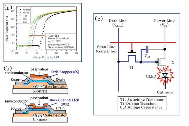
Fig. 1: (a) Gate-voltage vs. drain-current chart represents the evolution of a transfer curve as a function of bias-temperature-illumination stress. (b) The schematics of etch-stopper (ES) and back-channel-etch (BCE) structures are illustrated. (c) This conventional pixel design for an AMOLED panel uses two transistors and one capacitor.
Unfortunately, as mentioned above, the degradation of oxide TFTs is unavoidable under stress conditions. While the variation of µfe and Vth is less important in an AMOLED switching transistor, the current-induced threshold-voltage shift should be seriously considered for AMOLED driving transistors. It has been reported that a Vth shift of the driving transistor by 0.1 V induces variations in the resulting luminance of the OLED pixels by approximately 20%, which reflects the fact that the brightness of each pixel strongly depends on the drain current.14 Therefore, OLED displays should employ complex compensation circuits that have four or more TFTs, such as 4T2C, 5T2C, and 6T2C circuits, with 4T2C meaning that the circuit involves four transistors and two capacitors.3 In addition, an oxide semiconductor exhibits n-type-like properties, indicating that the major carrier in a channel is an electron. In an average OLED pixel circuit, a compensation circuit such as that shown in Fig. 2 should be employed in order to utilize n-type oxide TFTs, unlike the case for p-type LTPS TFTs, where this is not required.
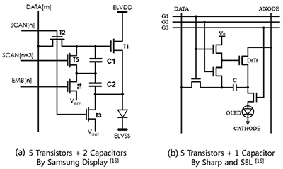
Fig. 2: This circuit diagram of a pixel (AMOLED panel based on a-IGZO TFTs) shows examples from (a) Samsung Display and (b) Sharp and Semiconductor Energy Laboratory (SEL).
Low-Resistivity Electrodes
Regarding large-sized AMOLED panels, the proper material for gate, source, and drain electrodes must be chosen. Large, high-resolution, and fast-frame-rate panels require electrodes with low resistivity, such as Al and Cu. However, Al has poor adhesion and easily oxidizes during the AMOLED processes. The Cu element easily diffuses and incorporates into the oxide semiconductor and gate insulator through thermal annealing and electro-migration, as is well-known, while showing the degradation of electrical properties such as mobility and stability. Recently, AUO applied Ti/Al/Ti electrodes to 37-in. AMLCDs, and Samsung Electronics applied Cu-based bus lines to a 15-in. AMLCD.17,18 Also, LG Display has adopted Cu-based electrodes in its 55-in. AMOLED-TV product.
Oxide-TFT Prospects for AMOLED TVs
From a market perspective, some observers in the display industry have deep concerns about the competitiveness of AMOLED TV based on oxide TFTs. As shown in Table 1, oxide semiconductors have promising possibilities; these initially led to a great deal of attention. Phrases such as “low-cost-based AMOLED backplane technology” or “like amorphous-silicon (a-Si:H) TFT technology for AMOLEDs” were used to describe progress toward the commercialization of AMOLED TV panels. Today, many companies have struggled to reduce fabrication costs in order to compete not only with AMOLED TV panels based on LTPS TFTs, but also with high-quality active-matrix liquid-crystal-display (AMLCD) TV panels based on a-Si:H TFTs.
Table 1: Shown is a comparison of AMOLED panel designs based on polysilicon, amorphous silicon, and oxide TFTs.
| AMOLED Panel |
Poly-Si TFT |
a-Si:H TFT |
Oxide TFT |
| Semiconductor |
Poly-crystalline Si |
Amorphous Si |
Amorphous IGZO |
| TFT uniformity |
Poor |
Good |
Good |
| Pixel circuit |
Complex (5T + 2C etc.) |
Complex (4T + 2C, 5T + 2C) |
Simple/Complex (2T + 1C/6T + 2C) |
| Channel mobility |
~100 cm2/V-sec |
1 cm2/V-sec |
>10 cm2/V-sec |
| TFT type |
PMOS (CMOS) |
NMOS |
NMOS |
| TFT mask steps |
5 ~ 11 |
4 ~ 5 |
5 ~7 |
| Cost/Yield |
High/Medium |
Low/No data |
Low/Medium |
To minimize the fabrication cost of an active-matrix backplane, it is important to reduce the number of photolithography masks. Current a-Si:H LCDs employ 4–5 masks, using a gray mask (also called a halftone mask) to pattern the source/drain electrodes and the channel in a single mask step. Samsung Display recently demonstrated AMOLED displays based on oxide TFTs, employing seven masks with an ES structure.19
As mentioned above, the ES-type device not only has superior stability, but also has excellent uniformity in the electrical properties because the ES layer can prevent the degradation of active layers during the following dry- or wet-etch process. The ES process in oxide TFTs is the contradictory factor with regard to fabrication cost and production yield. Thus, Sharp and LG Display have demonstrated mass-produced AMLCD and AMOLED backplanes with ES-type structures to guarantee the quality of the panels with uniform device performance. However, these companies have intensively developed a process with fewer mask steps (e.g., a BCE-type structure), resulting in a high-selective wet-etchant and self-passivation layer. To balance fabrication cost and yield in large-sized AMOLED displays, a BCE-type
device may be an inevitable selection. While the high-quality gate-insulator process may deteriorate the uniformity and performance of devices by damaging the active layer, a top-gate device configuration can be a possible solution in reducing the number of masks and parasitic capacitance for large-sized AMOLEDs.
Oxide TFT: A Solution Awaiting Solutions
Since small-sized AMOLED displays have been successful in the display marketplace, there is no doubt that AMOLED displays have the potential to become a superior display technology for TV. However, as far as the backplane technology is concerned, it is not yet clear which technology is suitable for large-sized AMOLEDs. Since 55-in. AMOLED TV panels were first demonstrated in 2012, many manufacturers and researchers have struggled to realize solutions to the following problems: mobility,
stability, and yield.
Recently, some research groups have reported a c-axis-aligned IGZO layer as a robust active layer, a large-sized (over Gen 8) sputtered target, and a high-mobility oxide material such as InZnSnO. Although device degradation and electronic-conduction mechanisms have been investigated in oxide TFTs, interdisciplinary researches from theoretical calculation to device engineering have increased drastically in recent times. As we gain deeper understanding into oxide semiconductors and processes, they will no doubt become the solution to realizing large-sized AMOLED TVs in the marketplace.
References
1K. Nomura, H. Ohta, A. Takagi, T. Kamiya, M. Hirano and H. Hosono, Nature 432, 488 (2004).
2J. S. Park, W. J. Maeng, H. S. Kim and J. S. Park, Thin Solid Films 520, 1679 (2012).
3T. Kamiya, K. Nomura, and H. Hosono, Sci. Technol. Adv. Mater. 11, 044305 (2010).
4J. K. Jeong, Semicond. Sci. Technol. 26, 034008 (2011).
5S. I. Kim, C. J. Kim, J. C. Park, I. Song, S. W. Kim, H. Yin, E. Lee, J. C. Lee, and Y. Park, IEEE Electron Device Meeting (IEDM 2008), 1 (2008).
6J. K. Jeong, H. W. Yang, J. H. Jeong, Y. G. Mo, and H. D. Kim, Appl. Phys. Lett. 93, 123508 (2008).
7J. H. Shin, J. S. Lee, C. S. Hwang, S. H. K. Park, W. S. Cheong, C. W. Byun, J. I. Lee, and H. Y. Chu, J. ETRI 31, 62 (2009).
8K. H. Lee, J. S. Jung, K. S. Son, J. S. Park, T. S. Kim, R. Choi, J. K. Jeong, J. Y. Kwon, B. Koo, and S. Lee, Appl. Phys. Lett. 95, 232106 (2009).
9J. Y. Kwon, K. S. Son, J. S. Jung, K. H. Lee, J. S. Park, T. S. Kim, K. H. Ji, R. Choi, J. L, Jeong, B. Koo, and S. Lee, Electrochem. Solid-State Lett. 13/6, H213 (2010).
10J. S. Jung, K. S. Son, K. H. Lee, J. S. Park, T. S. Kim, J. Y. Kown, K. B. Chung, J. S. Park, B. Koo, and S. Lee, Appl. Phys. Lett. 96, 193506 (2010).
11S. I. Kim, S. W. Kim, C. J. Kim, and J. S. Park, J. Electrochem. Soc. 158 (2), H115 (2011).
12H. S. Kim, et al., Appl. Phys. Lett. 97, 102103 (2010).
13K. H. Ji, et al. Appl. Phys. Lett. 98, 103509 (2011).
14H. J. In and O. K. Kwon, IEEE Electron Device Lett. 30, 377 (2009).
15Y. G. Mo, M, Kim, C. K. Kang, J. H. Jeong, Y. S. Park, C. G. Choi, H. D. Kim, and S. S. Kim, SID Symposium Digest Tech Papers 40, 37 (2010).
16T. Tanabe, S. Amano, H. Miyake, A. Suzuki, R. Komatsu, J. Koyama, S. Yamazaki, K. Okazaki, M. Katayama, H. Matsukizono, Y. Kanzaki, and T. Matsuo, SID Symposium Digest Tech. Papers 42, 88 (2012).
17M. C. Hung, et al., 2010 Intl. Workshop on TAOS, Tokyo, Japan.
18J. H. Lee, et al., SID Symposium Digest Tech. Papers 40, 625 (2010).
19H. D. Kim, J. S. Park, Y. G. Mo, and S. S. Kim, 9th Intl. Meeting on Information Displays, 3-1 (2009). •
Jin-Seong Park is a professor at Hanyang University. His research focuses on oxide-semiconductor materials and devices, flexible AMOLEDs, and thin-film encapsulations. He can be reached at jsparklime@hanyang.ac.kr.