SID Bay Area Chapter Hosts a Glimpse into the Future of Displays
by Stephen P. Atwood
The flyer headline read: “SID Bay Area Announces First One-Day Technical Conference: Display and Touch Technologies of the Future: Jan 16, 2013.” So, there I went to attend the first of what I sincerely hope will be an annual event, held in one of the most fertile technology innovation regions in the world. The program was expertly arranged by conference co-chairs Jennifer Colegrove and Rashmi Rao, and I was expecting a small gathering of about 50 or so die-hard display folk. What I encountered instead were over 160 attendees, a virtual sell-out, representing 43 different technology companies and countless different product and display-application interests. What unfolded throughout the day was a wonderful balance of speaker presentations, audience questions, panel discussions, and informal interactions that surely sparked some fresh ideas and seeded some new energy back into our industry.
Keynote speaker Jeffrey Han (Fig. 1) talked about his background at Perceptive Pixel, the company he founded. He described how his effort to create new touch-screen hardware quickly became an endeavor to expand the potential of multi-touch through software as he realized how little capability existed in user interfaces at the time. Now that Jeff as well as his company are part of the Microsoft Office organization, Perceptive Pixel remains a hardware division with a mission to seed interactive large-screen displays into every possible application, not just conference rooms and presentation arenas.
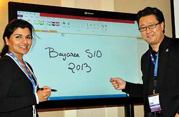
Fig. 1: Conference organizer Rashmi Rao and Perceptive Pixel Founder Jeff Han demonstrate the large-area multi-touch Perceptive Pixel touch screen.
Repeating a mantra we all know well, Jeff stressed that there is no perfect touch technology for all applications. In fact, Jeff explained that in his view, “Touch is not as good at content creation [as other methods],” and he went on to show some great demonstrations of how the future will be focused on pen and touch working together. For example, in a large-screen application, you might use your left hand for manipulation of the documents and windows and your right hand to draw and write the content.
Modality is also a big problem for touch applications – it’s challenging to program the computer to know what you intend when you use your fingers. However, we can use tools to define modality, such as pens for inking content and hands for manipulation. In a good UI design, your hand should be able to rest on the screen while you are inking and you should be able to perform a variety of content creation and context management tasks with no modality switching involved. This is part of what Jeff is working on at the Microsoft Research Center and it is surely a glimpse of what we’ll see in Microsoft products someday soon.
In the LCD Technology session, we heard from three speakers whose endeavors and those of their companies are all making fundamental contributions to the field. Candice Brown Elliott, founder of first Clairvoyant and now Nouvoyance, companies dedicated to innovative ways of producing multi-primary color with improved power efficiency and visual performance, presented her vision of key technology trends that are changing the landscape of color displays. “Thank goodness we’re moving to 4K resolution displays,” she began, talking about all the experiential advantages that users will gain from the ultra-high-definition formats. She then made a compelling case for the adoption of multi-primary display formats such as red-green-blue-yellow-cyan, which allow a variety of color metamers and creative ways to process and render images with wider color gamuts while avoiding increases in energy requirements.
She then explained how local dimming – using segmented 2-D backlights that enhance dynamic range – can be augmented with field-sequential color rendering to also greatly expand the boundaries on color and produce high-dynamic-range displays. These methods are much more achievable on consumer displays today due to the very low cost of high-performance processors and the new standards coming for digital-content distribution. Of course, mentioning field-sequential topics invokes fear in technologists used to dealing with color-breakup artifacts and poor user response. Well, not to fear, because as Candice described, the display area can be
segmented into small zones where each zone has its own color map and usually much lower color-diversity requirements that, in turn, can be met with virtual primaries (mixes of the actual primaries) that are much less saturated and therefore less likely to produce color breakup in observers.
Professor John F. Wager from Oregon State University took the podium next and presented the technical merits and future potential of oxide thin-film transistors (TFTs) for a variety of display applications, especially where transparency is needed. This is new technology that is just beginning to appear in mainstream OLED and LCD panels, promising a host of advantages and performance improvements. The first published work on oxide TFTs appeared in 2003 and serious interest developed around 2007. TFTs made from oxides are accumulation-mode devices, where electrons flow source to drain with positive gate voltage and positive drain voltage.
Making an oxide TFT with good mobility is challenging because unlike silicon, you want to discourage polycrystalline structures in favor of amorphous. This is because of an effect called “carrier trapping,” which causes an overall reduction in mobility in polycrystalline states. However, some combinations of elements such as zinc-tin (ZnSn) can be made amorphous rather than polycrystalline. Today, we see great success using InGaZnOx (IGZO,) which is now in commercial
use and is described in several ID magazine articles of late.
The key advantages of oxide TFTs for LCD manufacturing include high mobility, fast refresh, and easy insertion into already existing a-Si plants. By contrast, poly-Si fabrication requires a totally new plant, while oxide technology needs more of an upgrade. Oxide-TFT technology promises to spread into AMLCDs, EPDs, and AMOLEDs. It’s not yet ready to become part of flexible displays, but to read about progress being made in this area, see the article “Oxide TFTs for AMOLED TVs” in this issue. Also, see Fig. 2, for a comparison.
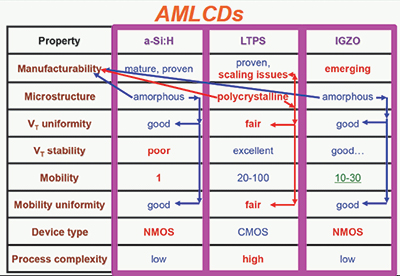
Fig. 2: John Wager presented this slide comparing the relevant properties of a-Si, low-temperature polysilicon (LTPS), and IGZO for AMLCD TFT fabrication. Credit: John F. Wager, “Amorphous Oxide Semiconductor Thin-Film Transistors for Display Applications,” presented at the Bay-Area SID Chapter’s One-Day Conference on “Displays and Touch Technologies of the Future,” Sunnyvale, CA, January 16, 2013.
Rounding out this trio of speakers was Seth Coe-Sullivan, CTO and co-founder of QD Vision, a company well known for its work in quantum-dot research, especially by those of us in the Northeast U.S. Seth discussed his company’s newest innovation, which involves LCD color-gamut-enhancing films with quantum-dot technology that can be installed directly into edge-lit backlights. This technology uses blue LEDs and then converts the blue-light energy into very specific spectrums of red, green, and blue as desired. QD Vision calls this technology “Color IQ,” and it was jointly announced with Sony at CES as the innovation behind Sony’s new “Triluminous” Displays. The result is what Seth describes as “LCDs with OLED color gamuts.” Seth went on to explain that another advantage of quantum dots is that they have worldwide environmental compliance, containing no materials that are known to be hazardous to the environment. In the first embodiment, Color IQ is packaged in a polymer film, but in the future quantum dots might be suitable for inclusion in the LED package itself, eliminating the need for an additional component. This could represent a sub-$100 solution to the panel designer.
However, there are further development challenges, including increasing total light output, managing heat, and improving lifetimes. Earlier QD optical performance used to degrade significantly at temperatures above 80°C but now is within ±3% up to 140°C. The currently expected lifetimes are greater than 2500 hours at power densities up to 100s of W/cm2 with no measureable luminance decay. Seth also believes that while the dots themselves are currently made in “batches,” the process itself is completely scalable to high-volume LCD manufacturing.
The next series of presentations focused on OLED technology, leading off with Dennis Kondakov, Principal Scientist at Dupont. Dennis, who compared two options for deposition of OLED materials onto backplanes during OLED manufacturing – evaporation with masks or solution printing and processing. Major considerations in selecting one of these processes include material waste and panel size because OLED materials are very expensive and processes must scale effectively to very large substrate sizes. Dupont believes that nozzle printing will be the approach chosen most often in future because of inherent advantages with the nozzles’ high printing rates of 2–5 m/sec and scalability.
Up next was Sean Xia, a research manager with Universal Display Corp., who discussed the short- and long-term potential for phosphorescent OLEDs (PHOLEDs). Xia and his team believe PHOLED materials hold the key to a variety of new innovations in displays as well as lighting applications, owing in large measure to the potential advantage in internal quantum efficiency (IQE) of up to 4× that of fluorescent OLEDs. This higher optical efficiency naturally reduces heat dissipation in the devices and allows many more creative design concepts than current lighting technologies. Of course, there are numerous advantages to both inorganic as well as organic LEDs for lighting, including wide color gamuts and high optical efficiency, but OLED and particularly PHOLED materials can be printed in large sheets and on
many types of flexible substrates while achieving tested performance up to 70 lm/w for 30,000 hours or longer. OLED lighting has been talked about before at conferences and in ID, but I was convinced that significant progress is being made, and it’s inevitable that we will see this technology in lighting applications in the not too distant future.
While UDC has been working on large-area OLEDs, Amal Ghosh and his colleagues at eMagin Corp. have been working on OLED microdisplays, packing more and more active-matrix RGB pixels onto silicon backplanes with display diagonals in the range of from 0.5 in. to about 0.9 in. Their most stunning achievement is a 0.86-in.-diagonal WUXGA microdisplay with an astounding 7,138,368 RGB pixel elements on it. This translates into a pixel pitch of about 9.6 µm, with each subpixel having dimensions of 3.45 × 8.5 µm. The application enables full HD 3-D glasses that can be used to create a virtual display experience. With the prototype the people from eMagin discussed, the diagonal field of view was 65°, creating a virtual image of approximately 212 in. on the diagonal at 12 ft.
with a luminance of over150 cd/m2. Because it is OLED technology, it has a very fast intrinsic response time and therefore can deliver full 3-D stereo images without flicker, motion blur, or image latency. And, of course, Ghosh promised they are also working on 2K × 2K imagers and beyond.
By this point, you might think we have already covered a full day but, in fact, all the above was presented before lunch! The afternoon sessions began with a keynote from Achin Bhowmik, Intel’s Director of Perceptual Computing, who characterized the major weakness of computers today as their limited ability to interact with humans. Although the human brain has a much slower processing speed than even the slowest computers, it can perform massive amounts of parallel processing on
multiple sensor inputs at the same time, creating a much broader range of analytical abilities than computers. Intel’s focus is to bridge that gap in a series of steps, starting by enabling touch interfaces in all forms of tablets and handheld devices.
As touch and Windows 8 become pervasive, Intel envisions moving to the next level with a system it calls “Perceptual Computing,” which is powered by a multi-input 3-D camera system and an SDK that Intel is currently offering for free in beta form. This SDK supports several perceptual modes, including Close-Range Interactions, Hand and Finger Level Tracking, Face Analysis, Tracking and Recognition, Speech Recognition, and 2-D/3-D Object Tracking. As Bhowmik said, this new approach “opens a world to creating applications without developing underlying controls.” You can see an interesting demo of these new concepts at
http://software.intel.com/en-us/vcsource/tools/perceptual-computing-sdk
These demos are more interesting than anything I can write about here in a short space. Clearly, we have seen for several years increasing interest all over the
industry in new types of 3-D and non-contact interaction modes with computers. Many concepts have recently been discussed at Display Week presentations, some built on the Microsoft Kinect platform. In fact, Intel’s product is compatible with the Kinect device as well as its standard depth camera offering, but the Intel SDK focuses on hands and faces rather than the entire body. “If we want computers to be interactive with people, we need to give people the tools to communicate with them,” said Bhowmik in closing.
Next, we heard from well-known industry expert Geoff Walker, who spoke about the future of touch technology. Noting that early sales of Windows 8 have not been encouraging, Geoff said there is a lack of hardware that fully enables the new features and that Windows 8 will soon drive the consumer market as hardware catches up. He also predicted that by 2018, 95% of phones will be touch enabled – something I’m not at all surprised about. Recently, the concentration of touch in some notebook formats such as All-in-Ones (AiOs) actually went down due to fears of pro-cap-only choices for Windows 8 – not because the market doesn’t exist. Similarly, with traditional “clamshell” notebooks, increasing touch penetration will require solutions that are easier or more convenient than alternative input methods and, of course, Windows 8!
Meanwhile, Geoff said that large-format touch has huge opportunities, and there are a number of technology options on the market or coming to market soon, including: camera-based, vision-based, FTIR, projected-capacitive (Pro-Cap), “traditional” infrared, and high-finger-count multi-touch infrared. All of these are in various stages of development or deployment now. Not surprisingly, Pro-Cap is the biggest show in town, capturing 83% of the market for screen applications less than 15 in. and spawning a number of R&D efforts on core materials such as metal mesh, silver nanowires, carbon nanotubes, and conductive polymers. However, as Geoff explained, it’s really the process to manufacture these screens that determines cost and performance improve-ments. With the OEM cost of a 13.3-in Pro-Cap screen in the range of $55–85, there have clearly been many improvements recently.
The other trend that Geoff emphasized was renewed interest in stylus input. Windows 7 was finger-focused because of the perceived failure of stylus input on
tablet PCs. However, several recent products have brought back the stylus, which is much better for content creation such as drawing and writing, so Window 8 will
likely re-energize stylus input. In fact, the ideal embodiment on larger screens may be just what Jeff Han discussed earlier: hand recognition for control of frames and windows and simultaneous stylus input for actual content creation.
Next in line was Joel Kent from Elo TouchSystems to explain how surface-acoustic-wave (SAW) technology may be seeing a rebirth. He explained his company’s new edge-to-edge SAW implementation, which can produce a virtually bezel-less design with the sensors and transducers moved to the back of the glass. Until recently, the touch market was predominantly a commercial and industrial application space. As we know, beginning around 2000, the consumer touch market began its expansion
way beyond the commercial market. This is important because the user’s learning curve in the two markets is very different. Consumers will make the effort to learn how to best optimize their personal devices, but commercial market users are transient and will not invest time to learn; therefore, the touch interface and application experience must still be significantly different. Examples Kent cited included an airport check-in kiosk vs. a smartphone.
Rounding out the trio of touch technology speakers was Zachi Baharav, Manager of R&D from Corning. We’re all familiar with the significant and highly innovative role Corning has played in the LCD industry for the last 30+ years, but it was interesting to hear how diverse and nuanced the company’s offerings are for touch-sensor development. The diversity in touch-application requirements varies in strength, thickness, chemistry, tolerance to processing, surface texture, etc., in much greater degrees than we might have realized. Baharav brought with him some of the best Corning videos, including the famous “A Day Made of Glass.” Famous for their imaginative depictions of transparent tablet displays and augmented reality, these videos pose many interesting questions about user
interaction as well as future modalities for information devices. They are, incidentally, also available on youtube but they are more fun to watch on the big screens at a conference like this one.
The final round of talks addressed flexible displays and emerging technologies. Jennifer Colegrove, President of Touch Display Research, spoke about the opportunities for continued technical advances in technologies and commented on the future potential. She said that there are “currently over 10 different technologies that can be made into flexible displays.” She went on to make a bold prediction that we will see a “…flexible AMOLED from Samsung in 2013 that will be a phone and a tablet combined, with a screen size >5 in.” That certainly got my attention! The market revenue for flexible displays in 2011 was a modest $400 million (which is larger than I would have even thought), but Jennifer predicts by 2015 that it could be as much as $2.5 billion Some of the key technology areas that are ripe for further development include OLED flexible barrier layers, color for e-Paper, ITO replacement materials, flexible touch, and better/smaller batteries.
The last speaker was Jian Chen, VP of R&D for Nanosys, a former winner of SID’s prestigous Display Industry Awards. Dr. Chen explained that green LED efficiency was one of the factors limiting adoption of RGB LED backlights. Also, differential aging made it hard to maintain white balance over long product life cycles, which explains why phosphor white LEDs have become the de-facto standard for most LED backlight designs. Nanosys provides a film for LCD backlights it calls QDEF, which produces a secondary light emission with quantum-dot technology. These films can be tuned to very specific light wavelengths based on stimulation from 365-nm blue LED sources. Nanosys has demonstrated its process to be very scalable with modest investment, allowing it to partner with companies such as 3M to produce a roll-to-roll manufacturing process. This ensures the product can meet the demands of major LCD-manufacturing customers.
While a great many seemingly diverse topics were covered during the course of this event, it was clear that they all fit together when you step back and try
to envision the characteristics of display technology several years into the future:
• More advanced and efficient interaction between people and their devices.
• A wider range of power-efficient, lower-cost, and even flexible devices going way beyond what we have today.
• Displays becoming more fully integrated into all our appliances and devices, with virtual linkage creating a seamless environment for information exchange.
• And best of all, a wide range of new opportunities for invention, discovery, investment, and future careers.
I really enjoyed my trip to the future and it was all due to the outstanding efforts of the BA chapter conference team pictured in Fig. 3. Congratulations to them all for a very successful conference! •
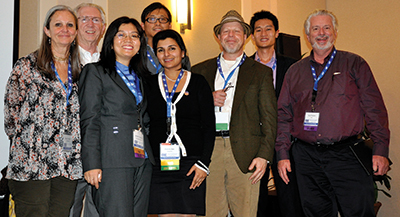
Fig. 3: Bay Area SID Chapter Conference Organizers. From left to right in back row: Joel Pollack, Steven Huang, and Cheng-Wei Pei; from left to right in front row: Carolyn Marsden, Jennifer Colegrove, Rashmi Rao, John Miller, and Geoff Walker.