A preview of some of the most interesting papers appearing in the
December 2008 issue of the Journal of the SID.
To obtain access to these articles on-line, please go to www.sid.org
Edited by Aris Silzars
Inorganic EL devices with high-performance blue phosphor and application to 34-in. flat-panel televisions
Hiroki Hamada (SID Member)
Isao Yoshida (SID Member)
Don Carkner
Xingwei Wu
Masaki Kutsukake
Kumpei Oda (SID Member)
Sanyo Electric Co., Ltd.
Abstract — A high-performance inorganic electroluminescence (EL) device has been successfully developed by using an EL structure with a thick dielectric layer (TDEL) and sputtered BaAl2S4:Eu blue phosphor. The luminance and efficacy were higher than 2300 cd/m2 and 2.5 lm/W at L60, 120 Hz, respectively. Furthermore, the luminance at L60, 1.2 kHz was more than 23,000 cd/m2. The phosphor layer has a single phase and a highly oriented crystalline structure. The phosphor also shows high stability in air. A 34-in. high-definition television (HDTV) has been developed by combining a TDEL structure and color-conversion materials. The panels with an optimized color filter demonstrated a peak luminance of 350 cd/m2, a color gamut of more than 100% NTSC, and a wide viewing angle similar to that of plasma-display panels. The high reproducibility of the 34-in. panels using our pilot line has been confirmed.
Figure 1 shows the schematic structure of a TDEL device. The TDEL device has a thick dielectric layer, which replaces the thin dielectric layer of TFEL devices. The thick dielectric layer is prepared by combining the screen-printing method and firing process without using any vacuum processes. The thick dielectric layer consists of materials with high dielectric constants.
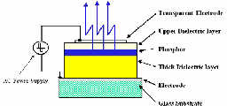
FIGURE 1 — Schematic drawing of the TDEL structure.
Molecular design for stabilizing a blue phase III and electro-optical switching in the blue phase
Atsushi Yoshizawa
Hirosaki University
Abstract — The molecular design of a liquid crystal to stabilize a blue phase III (BPIII) is reviewed, and the electro-optical switching with a response time on the order of 10–2 sec for BPIII exhibited by a novel chiral liquid crystal is reported. Binaphthyl derivatives and T-shaped compounds are presented, and the structure–property correlations of the chiral compounds are discussed. Two origins of the twisting power of the compounds, i.e., their inherent molecular chirality and the chirality-induced twist conformation, play an important role in the appearance of the BPIII. Furthermore, BPIII was also induced in some binary mixtures of a host nematic liquid-crystal possessing molecular biaxiality and a conventional chiral compound. The electro-optical switching in the BPIII is attributed to an electric-field-induced phase transition between the BPIII and nematic (N) phases. BPIII is on the microscopically twisted nematic order, but is macroscopically isotropic. Therefore, the present technology can offer a pronounced black state in the BPIII without surface treatment and a homogeneous bright state in the induced N phase.
The appearance of blue phases results from the competition between the chiral twisting force and the desire for molecules to fill space uniformly. Although many types of liquid crystals have been prepared, molecular design for stabilizing blue phases has never been obtained. Theoretical work suggests that biaxaility plays an important role in the blue phases. However, the biaxiality in most chiral nematic liquid crystals is slight, and as a result the double-twist structure cannot exist in a wide temperature range.
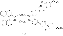
FIGURE 1 — Molecular structure of the binaphthyl derivative 1 – n.
Effects of display properties on perceived color-gamut volume and preference
Masato Sakurai (SID Member)
Rodney L. Heckaman
Stacey E. Casella
Mark D. Fairchild (SID Member)
Takehiro Nakatsue (SID Member)
Yoshihide Shimpuku (SID Member)
Sony Corp.
Abstract — The effect of varying the color gamut of an extended-gamut LCD on color appearance and preference was measured psychometrically in two experiments at each of two separate laboratories over a representative set of 10 images each. The first experiment measured the effect of color gamut on appearance, and the effect on the appearance attribute colorfulness was shown to be relatively strong compared with other attributes as the volume of display color gamut is varied. Overall, colorfulness monotonically increased at constant sensitivity as the gamut area in xy chromaticities increased while tending to become less and less sensitive to increasing the gamut volumes in CIELAB and CIECAM02. In the second experiment, the overall preference indicated an optimal color gamut for the display gamut volume even though the results were shown to be highly scene-dependent.
Four versions of each scene were rendered to each of four sets of simulated display primaries with gamut volume factors of 1.0, 0.8, 0.6, and 0.4 times the full-color gamut of the display in CIELAB a*b* at Group-A and 1.0, 0.89, 0.77, and 0.63 at Group-B, respectively. All the versions were constrained to maintain both the display's white point and hue within the ability of CIELAB to maintain perceptual hue. Therefore, the lightness in each version of any given scene was rendered equally.
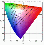
FIGURE 2 — Color gamut for the simulated primaries plotted on a u′v′ chromaticity diagram. The outside triangle indicates the full gamut of the display in this experiment.
High-performance MgO thin films for PDPs with a high-rate sputtering-deposition process
Masaharu Terauchi, Jun Hashimoto,
Hikaru Nishitani, Yusuke Fukui,
Michiko Okafuji, Hitoshi Yamashita,
Hiroshi Hayata, Takafumi Okuma,
Hitoshi Yamanishi, Mikihiko Nishitani,
Masatoshi Kitagawa
Panasonic AVC Networks Co.
Abstract — A high-rate sputtering-deposition process for MgO thin films for PDP fabrication was recently developed. The deposition rate of the MgO thin film was about 300 nm/min which shows the possibility of production-line application. The MgO film deposited in this work has a higher density than that of other deposition processes such as electron-beam deposition and shows good discharge characteristics including firing voltage and discharge formation. These were achieved by controlling the stoichiometry and/or the impurity doping during the sputtering process.
To improve the uniformity of the film thickness, a groove in the target was made. Figure 3 shows a photograph of the target with a grooved circle. It was shown that the groove in the target was made to be incandescent and the other part of the target was not incandescent in sputtering. By making the groove, the incandescent part of the target can be controlled. So, the uniformity of the film thickness was improved within ±10% in the 10-cm square.
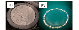
FIGURE 3 — Photograph of the target with the circled groove: (a) Before discharging, (b) discharging.
Use of self-erase discharges for high-speed and low-voltage addressing of PDPs
Masakazu Shimura
Tsuyoshi Yamaguchi
Tomokazu Shiga (SID Member)
Shigeo Mikoshiba (SID Fellow)
University of Electro-Communications
Abstract — A technique called "self-erase-discharge addressing" has been incorporated with a address-while-display driving scheme, contiguous subfield, and erase addressing to obtain high-speed and low-voltage addressing of PDPs. The technique uses a relatively high X-sustain pulse voltage VXsus, which produces a weak self-erase discharge at its trailing edge. An application of a data pulse Vdata synchronous to a weak self-erase discharge results in full erase discharge and eliminates all the wall charges. The technique assures a wider operating-voltage margin since it provides identical amounts of priming charges as well as wall charges to all the horizontal scan lines just prior to addressing. The priming charges are generated by the weak self-erase discharges, resulting in low Vdata of 30 V and a high addressing speed of 0.66 μsec for a Ne + 10% Xe PDP. VXsus = 245 V, and the voltage margins of Vdata and VXsus were 35 and 16 V, respectively. For a 30% Xe PDP, Vdata and VXsus were 30 and 335 V, respectively, with an addressing speed of 1.0 μsec. In order to obtain high dark-room contrast, it is essential to use ramp reset pulses, with which erase addressing cannot be achieved. By adopting the write addressing only to the first subfield and the self-erase-discharge addressing to the subsequent subfields, a peak and background luminance in green of 3100 and 0.22 cd/m2, respectively, were obtained with a dark-room contrast of 14,000:1. The number of subfields was 28, and the light emission duty was 83%. The number of ramp reset pulse drivers could be reduced to 12 by adopting the common reset pulse technique.
Figure 4 shows a timing chart of the proposed driving scheme. There are a reset period and 32 subfields having a constant width of 512 μsec within a TV field time of 16.7 msec. Each subfield consists of an address period and a sustain period. The address period of one of the scan electrodes is provided within the display period of other scan elec-trodes, and hence the name address-while-display scheme. The number of sustain pulses in the respective subfields can be varied from 2 to 126. This allows for smooth gray scales even at low luminance levels.
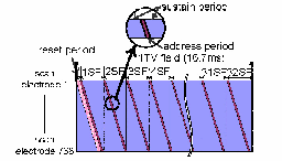
FIGURE 4 — Timing chart of self-erase-discharge addressing scheme.
Characteristics of ACPDP test panels with aluminum fence electrode formed via anodic bonding with soda-lime glass
Seog-Young Lee (SID Student Member)
Mi-Yeon Lee
Won-Yeol Choi
Dong-Heon Lee
Yong-Seog Kim (SID Member)
Hongik University
Abstract — In an attempt to reduce materials and processing costs of ACPDPs, aluminum fence electrodes were prepared on soda-lime glass substrates by chemically etching aluminum foil bonded directly onto the substrate via an anodic-bonding process. Several different fence-electrode patterns were designed and coated either with a glass dielectric layer or with an anodic aluminum oxide layer. Firing voltages, operation margin, luminance, and luminous efficiency of such test panels were evaluated. The results indicated that the performance of test panels with aluminum fence electrodes is comparable with conventional test panels with ITO/Ag electrodes, demonstrating the possibility of a dramatic reduction in the costs of ACPDPs.
Table 1 shows various types of aluminum fence electrodes prepared in this study. Type A is the typical fence electrode with shorting bars formed at the center of the cells. The fence width was 20 μm and the sustaining gap was 70 μm. Type B and C were designed to increase the electrode area near the sustaining gap and, therefore, intensify the glow discharge as in the in-bus structure. In those designs, the width of the fence at the sustaining gap was increased to 40 μm and the cell opening ratio of the cells was decreased by 11% for type B and 7% for type C, respectively. Type D was designed to maximize the area of the facing electrodes such that the firing voltage can be reduced further.
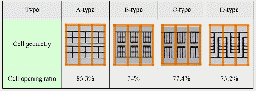
TABLE 1 — Geometry and cell-opening ratio of fence-type electrodes used in this study.
Ink-jet-printable phosphorescent organic light-emitting-diode devices
Takuya Sonoyama
Masaki Ito
Shunichi Seki
Satoru Miyashita
Sean Xia (SID Member)
Jason Brooks (SID Member)
Kwang-Ohk Cheon
Raymond C. Kwong (SID Member)
Michael Inbasekaran
Julie J. Brown (SID Member)
Seiko-Epson Corp.
Abstract — A novel method for the fabrication of ink-jet-printed organic light-emitting-diode devices is discussed. Unlike previously reported solution-processed OLED devices, the emissive layer of OLED devices reported here does not contain polymeric materials. The emission of the ink-jet-printed P2OLED (IJ-P2OLED) device is demonstrated for the first time. It shows good color and uniform emission although it uses small-molecule solution. Ink-jet-printed green P2OLED devices possess a high luminous efficiency of 22 cd/A at 2000 cd/m2 and is based on phosphorescent emission. The latest solution-processed phosphorescent OLED performance by spin-coating is disclosed. The red P2OLED exhibits a projected LT50 of >53,000 hours with a luminous efficiency of 9 cd/A at 500 cd/m2. The green P2OLED shows a projected LT50 of >52,000 hours with a luminous efficiency of 35 cd/A at 1000 cd/m2. Also discussed is a newly developed sky-blue P2OLED with a projected LT50 of >3000 hours and a luminous efficiency of 18 cd/A at 500 cd/m2.
Figure 9 shows the normalized EL spectra of the red, green, and the newly developed sky-blue P2OLEDs measured at 10 mA/cm2 and the 1931 Commission International de l'Eclairage (CIE) coordinates. The red P2OLED has a peak wavelength at 623 nm with coordinates of (0.66, 0.33). The green P2OLED has a peak wavelength at 521 nm with coordinates of (0.33, 0.63). The sky-blue P2OLED has a peak wavelength at 474 nm with coordinates of (0.19, 0.40). No cavity was used in this experiment to affect the emission.
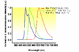
FIGURE 9 —Normalized electroluminescence spectra of red, green, and blue P2OLEDs with CIE coordinates of (0.66, 0.33), (0.33, 0.66), and (0.19, 0.40), respectively, measured at 10 mA/cm2.
Contrast gain and power savings using local-dimming backlights
Erno H. A. Langendijk (SID Member)
Remco Muijs (SID Member)
William van Beek
Philips Research Laboratories
Abstract — The contrast and power consumption of today's liquid-crystal displays (LCDs) can be improved substantially by introducing (local) dimming backlights. In fact, infinite dynamic contrast and power savings of well over 50% have been claimed for such displays. Because these claims are generally made for very specific backlight designs and image content, the contrast gain and power savings are quantified as a function of the number of backlight segments for a large variety of image content.
The number of segments (# segments) was the main independent variable. Two-dimensional quadratic Lorentz optical profiles of which the width was chosen in such a manner that the maximum luminance nonuniformity of a full white screen amounts to 1% were used. A static panel contrast of 1000, which is typical for today's LC panels, was scanned. The backlight drive values were established from the incoming video content using the Max(R,G,B) algorithm.
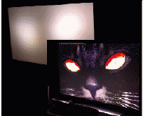
FIGURE 1 — Illustration of local dimming. The backlight (rear image) is at full brightness at the position of the cat's eyes and is dimmed at the darker parts of the image. The panel (front image) is simultaneously compensated for the backlight modulation such that the scene is properly depicted.
Full-color photo-addressable electronic paper using cholesteric liquid crystals and organic photoconductors
Haruo Harada (SID Member)
Makoto Gomyo
Yasunori Okano
Taijyu Gan
Chisato Urano
Yasuhiro Yamaguchi
Tomozumi Uesaka
Hiroshi Arisawa
Fuji Xerox Co., Ltd.
Abstract — Full-color photo-addressable electronic paper using cholesteric liquid crystals and organic photoconductors was developed. The electronic paper is comprised of two stacked photo-addressable elements displaying blue/green and red images, respectively. Each photo-addressable element was independently controlled by two different color-addressing lights. Furthermore, blue and green images were selectively switched by one organic photoconductor using the threshold characteristics of cholesteric liquid crystals. A highly reflective polymer-dispersed cholesteric liquid-crystal (PDCLC) layer was obtained by a new formation process based on the sol-gel transition behavior of a gelatin matrix and an agar overcoat layer. The PDCLC layer had a close-packed honeycomb-like monolayer structure with a flat surface. The A6-sized prototype had paper-like features and showed full-color bistable images instantly written with a viewer-type writing apparatus.
Figure 7 shows the formation process of the PDCLC display layers. Monodispersed ChLCs-in-water emulsion was obtained by a membrane emulsification technique. A membrane with a 4.4-μm pore size was used, and the average diameter of the obtained droplets was about 15 μm. The concentrated emulsion was mixed with an aqueous solution of acid-processed bovine bone gelatin to obtain a mixed emulsion containing 10.5 vol.% ChLC and 4.5 vol.% gelatin. The mixed ChLC-in-gelatin aqueous emulsion was applied to the substrate at a wet thickness of about 75 μm and was over-coated with a 1-wt.% aqueous solution of agar having a wet thickness of about 30 μm. Since this process was carried out at high tem-perature (60°C), both layers were in a low viscosity sol state.
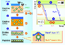
FIGURE 7 — Formation process of the PDCLC display layer. The close-packed honeycomb-like monolayer PDCLC is formed by using the differences in the sol-gel behavior between gelatin and agar.
A 5-in. flexible ferroelectric liquid-crystal display driven by organic thin-film transistors
Yoshihide Fujisaki
Hiroto Sato
Tatsuya Takei
Toshihiro Yamamoto
Hideo Fujikake (SID Member)
Shizuo Tokito
Taiichiro Kurita (SID Member)
NHK Science & Technical ResearchLaboratory
Abstract — An organic thin-film-transistor (OTFT) driven color flexible ferroelectric-liquid-crystal (FLC) display with 160 ´ 120 pixels and a resolution of 50 ppi has been developed. The flexible FLC was fabricated on a pentacene-OTFT array using printing and lamination techniques. To drive the display at a fast driving speed, an OTFT was developed with a short channel length having a large current output. The fabricated OTFT array with a channel length of 5 μm exhibits a carrier mobility of 0.3 cm2/V-sec and an ON/OFF ratio of over 107 at a low drain voltage of –6 V. A field-sequential-color system with a flexible backlight unit was also developed and used to drive the display. Color moving images were successively shown on the 5-in. display using an active-matrix driving technique of the OTFT.
The structure of the flexible FLC display is shown in Fig. 1. A composite film, consisting of the FLC and polymer fibers, is sandwiched between rubbed polyimide alignment layers on plastic film. Lattice-patterned polymer walls that adhere to the surface of the substrates are formed in the composite film. This structure provides high mechanical stability of the device in a bent state. The FLC molecules are mono-stabilized by the strong anchoring effect from the polymer fibers that lie in the rubbing direction of the polyimide alignment layers.
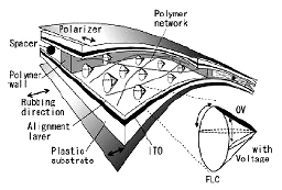
FIGURE 1 — Structure of a flexible FLC display panel.
Improved discharge time lag of address pulse in an ACPDP with auxiliary electrodes
Cheol Jang
Kyung Cheol Choi (SID Member)
Korea Advanced Institute of Science and Technology
Abstract — New driving waveforms are proposed for an ACPDP with an auxiliary electrode. Auxiliary pulses and a stepped scan pulse during the address period distinguish the proposed waveforms from conventional waveforms. The address discharge time lag in an ACPDP with auxiliary electrodes was improved by application of auxiliary pulses and a stepped scan pulse during the address period. The interaction between the auxiliary pulse and the stepped scan pulse generates priming particles directly prior to the address discharge, and these priming particles influence the address discharge. As a result, the firing voltage of the address pulseis lowered, and the minimum address voltage is lower than that of conventional driving waveforms. Experimental results confirm that the address discharge time lag of the proposed waveforms is 32% lower than that of conventional driving waveforms.
As shown in Fig. 1, the FEEL PDP has an auxiliary electrode between the sustain electrodes. When auxiliary pulses were applied to the auxiliary electrodes during the sustain period, the luminous efficacy was increased. The auxiliary pulses were applied between the sustain pulses, which were applied, in turn, to a common electrode and a scan electrode.
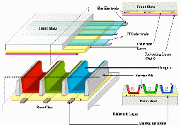
FIGURE 1 — Schematic diagram of an ACPDP with a coplanar gap of 200 μm and an auxiliary electrode.
Fault-tolerant display image-data-manipulation unit for system-on-panel
Hyun-Goo Lee
Jae-Hee You
Hongik University
Abstract — Bit-partitioned and conventional shifts, as well as type transformations of multimedia data, are frequently used for display image-processing systems. A data manipulation unit with fault-recovery capability based on redundancies is proposed for system-on-panel with low-processing technology yield. Utilizing data manipulations that are similar to normal shift operation, a proposed data-manipulation unit is designed with a few additional paths added to the existing barrel shifter. The design methodologies are verified with FPGA and the performance is evaluated in terms of the advantages.
The proposed DMU, as SOP technology evolves, can be integrated on the display panel. Also, since it is based on two 32-bit barrel shifters, it can be utilized in multimedia processors with more than two arithmetic units. Since the DMU is mainly composed of regular interconnections with higher yield compared to the devices, fault tolerance with redundancies and scaling can be easily realized.
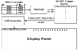
FIGURE 3 — The proposed DMU architecture.