The use of laser patterning on silver nanowire enables reduced manufacturing costs and increased flexibility for touch-panel manufacturers.
by Terry Pothoven
SINCE the introduction of Apple's iPhone, the market for touchscreen displays has grown swiftly to $16 billion and is expected to double by 2018. With the much anticipated release of Windows 8, the first Windows-based operating system designed with a touchscreen interface, that trend will accelerate. Against the background of rapidly increasing demand, manufacturers of touchscreens, seeking an advantage over competitors, continue to look for ways to improve performance, reduce costs, and increase output of touchscreen displays. Laserod Technologies has developed a high speed direct laser patterning process for a new and unique material called silver nanowire that addresses all of those objectives. The silver nanowire used in this development work is proprietary ClearOhm film provided by Cambrios Technologies of Sunnyvale, California.
Silver Nanowire
Silver nanowire is a nanostructured inorganic material that produces a transparent conductor coating that has advantages in flexibility, conductivity, and cost over widely used indium tin oxide (ITO). The silver nanowire material consists of a wet processable dispersion of high-aspect-ratio silver nanowires. Starting from silver salts, twinned-crystal silver nanowires are grown via the polyol process. By carefully controlling the process parameters, high aspect ratio silver nanowires can be synthesized at high yield, with an average diameter in the low tens of nanometers and an average length in excess of 10 μm. Independent control of nanowire length and diameter is possible, allowing the tailoring of morphology-dependent optical and electrical properties for specific applications. These nano-structures are then purified and formulated into a coatable suspension that is compatible with industry standard coating methods such as roll-to-roll slot die coating or spin coating.
The transparent conductive layer is created by coating the formulated suspension of nanowires on the surface of a substrate such as glass or plastic. Upon drying of the solvent, the nanowires form an interconnected, two-dimensional mesh on the surface. Controlling the sheet resistivity of the layer of interconnected nanowires is accomplished by changing the number density of nanowires on the surface. The electrical properties of the interconnected mesh are well described by the theory of percolation, in which the number density of nanowires required to achieve a continuously conductive path on the substrate scales inversely with the square of their length (N ~ 1/L2). Thus, high aspect ratio nanowires are uniquely suited to achieve high electrical conductivity with a minimal amount of metal.
Similar to ITO, silver nanowire can be applied to glass, polycarbonate, and PET films and can be used for many applications as a coating material for transparent electrodes for touch panels, liquid crystal displays, e-paper, OLED devices, and thin film photovoltaics. The key advantages of silver nanowire over ITO are flexibility, improved optical properties, and reduced manufacturing cost. Although the unit cost of indium is comparable to the cost of silver, the conductivity of silver is far superior to that of indium, requiring a small fraction of silver relative to the amount of indium needed for the same surface area and resulting conductivity. Additionally, silver nanowire is applied to material using a wet chemical solution and does not require the expensive vacuum application required by ITO.
When applied to PET film, silver nanowire coatings achieve some optical performance advantages over similar ITO coatings. As reported in an article in the January 2012 issue ofInformation Display magazine titled "Wet Processable Transparent Conductive Materials," the transmission of these films can be in excess of 90% at 40 Ω/sq. or > 98% for the conductive coating itself. Comparing this to ITO film that includes a multilayered anti-reflection coating, the silver nanowire film had an equivalent transmission at 50 Ω/sq. as compared to ITO film at a 3x higher sheet resistance. For standard-grade ITO film that does not include anti-reflection coatings, the transmission advantage of this film would be significantly larger.
In the laboratory experiments described below, which were conducted on PET substrates, Laserod Technologies used a high speed direct laser patterning process to produce invisible patterns in silver nanowire. The combination of laser processing with silver nanowire results in lower costs and increased manufacturing flexibility when compared to the industry standard of wet chemical etching on ITO. Most significant is the fact that silver nanowire coatings can be modified quite effectively with laser ablation once cured. Compared to wet chemical etching, the use of lasers reduces the cost by approximately 50% and eliminates the environmental impact associated with chemicals used in the etching process.
Laser Ablation Process
Direct dry etch processing, which uses a laser instead of chemicals to remove material, has been around for many years. Similar to wet chemical etching, laser ablation can remove microscopic lines in ITO that create isolated conducting patterns in the remaining ITO for applications such as linearization patterns and quasi-invisible conductor matrices in touch screens. Dry etch processing does not require the toxic chemicals used in the wet chemical etching process and does not require expensive masks to make complex patterns in ITO. Historically, the laser beam in direct dry etch was directed straight down to a production part secured to an X/Y stage. A computer program moved the X/Y stage to scribe the desired pattern on the part. The process provided flexibility for research and development purposes, but lacked the throughput speed necessary for cost-effective volume manufacturing. The speed was typically limited by the power of the laser.
Advances in laser technology in the last 5 years have made it possible to increase production throughput with higher powered lasers and galvanometer beam-delivery systems. Modern lasers now produce per pulse energies and repetition rates that exceed the speed of the fastest X/Y stage. Laserod integrates high powered lasers with galvanometer beam-delivery systems to rapidly ablate complex patterns on glass and PET. The position of the part remains fixed. The galvanometer uses two overhead moving mirrors to direct the laser beam in the desired ablation pattern. The process avoids moving significant mass and only requires movement of the mirrors, thereby allowing the laser beam to move across the part at speeds as high as 12 m/sec. For typical touch-panel applications, increased production rates by means of laser patterning, combined with the elimination of expensive masks and chemicals, now enables a very cost effective and green production process.
Comparing Laser Wavelengths
Laserod used both diode-pumped and fiber-based laser systems to compare three of the most common laser wavelengths (1064 nm infrared, 532 nm visible, and 355 nm ultra-violet). Each wavelength was reviewed to compare laser patterning speed, electrical isolation, and visibility of the patterned material. Each of these three factors directly relates to throughput, yield, and transparency. Using an array of laser power, repetition rate, spot size, and speed, the company produced a test matrix to analyze the results. Several solid-state lasers (the Coherent Avia series, the SPI SM series, and the Lee Laser LDP series) were used to process the samples. Table 1 shows some of the test values.
Table 1: These wavelengths all produce low-visibility patterns.
| Laser Wavelength (nm) |
Laser Power (W) |
Laser Patterning Repetition (kHz) |
Electrical Rate/Speed (m/sec) |
Isolation (GΩ) |
| 1064 |
5.25 |
150 |
4 |
> 1 |
| 1064 |
12 |
400 |
12 |
> 1 |
| 532 |
0.57 |
15 |
0.3 |
> 1 |
| 532 |
1 |
100 |
1 |
> 1 |
| 355 |
1.2 |
220 |
4.5 |
> 1 |
Electrical Isolation
The team observed during the experiments that each wavelength easily obtains very high electrical isolation, the fundamental requirement of typical laser-based patterning applications. The absolute limit of isolation could not be determined because the equipment used at the time of processing was limited to a range of 1 GΩ. However, this isolation level is more than adequate for most patterning applications.
Process Speed
Based on the values obtained and those extra-polated from laser engines available, it is clear that using an infrared laser engine produces the highest processing speed. Using the IR laser, speeds in excess of 12 m/sec were achieved with good isolation. These extremely high speeds can typically only be used in simple straight-line laser processing applications. More complex patterns require the use of a lower patterning speed (3–6 m/sec), due to the limitations of current state-of-the-art laser patterning beam delivery systems. This represents a big change from past history. Five years ago, laser engines were not yet production tested or proven to produce sufficient laser energy at high repetition rates to support high speed laser-beam deliveries. After a big push from laser companies to increase power levels at high repetition rates, this problem has been resolved. Based on the beam delivery limitations for typical patterning applications, all three wavelengths were found to be capable of supplying sufficient power to create isolated patterns at speeds of 3–6 m/sec.
Figure 1 shows a typical smartphone pattern that the author has used to illustrate the speed of laser patterning. In the past, this pattern would have taken 10 sec to create in ITO. Maximum patterning speed is limited by insufficient absorption of the laser energy into the ITO, which results in substrate damage when using plastics. This effect limits the amount of laser energy that can be used and thus the maximum speed. Even with this limitation, laser patterning is still a very production-competitive process. Using silver nanowire, Laserod was able to reduce the process time to 7 sec and achieve electrical isolation with no damage. This was due to the higher absorption of the laser energy by the silver. A customized beam-delivery system could reduce this patterning time to 5 sec or less.
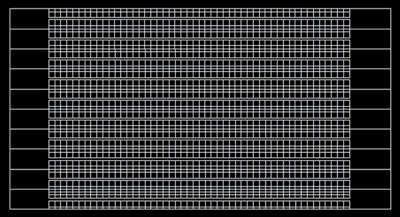
Fig. 1: A typical smartphone touch panel electrode pattern would take 10 sec to create in ITO, but took 7 sec with silver nanowire.
Visibility – or Lack Thereof
The research team next moved to a dark-field microscope. This instrument produced high quality images that enabled a comparison of the visibility of the lines. Those lines patterned using ultraviolet laser pulses tended to damage the topcoat (Fig. 2) at the power levels required for good electrical isolation. They also showed more melting of the silver nanowire (Fig. 3), which creates very reflective surfaces. These two features made it very easy to detect the lines with the naked eye, once the sample was reviewed under dark background and bright lighting.
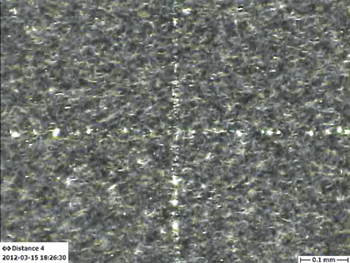
Fig. 2: The lines patterned using ultraviolet laser pulses tended to damage the topcoat.
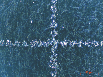
Fig. 3: The ultraviolet laser pulses also melted the silver nanowires.
Once sufficient energy was obtained to create electrically isolated lines in the silver nanowire, using visible laser light, damage to the PET substrate in the form of heat marks was observed(Fig. 4). However, after several rounds of optimization of the optics to obtain the best energy density on the material, invisible lines with electrical isolation were produced (Fig. 5).
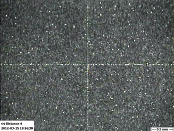
Fig. 4: Faint heat marks can be seen in this pattern due to energy absorbed in the PET substrate by the laser.
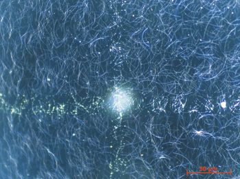
Fig. 5: Here, PET damage has been reduced to the point where it cannot be detected by the naked eye.
Infrared laser light was found to be ideal for producing invisible lines with no damage. Figure 6 shows a macro view and Fig. 7 a micro view. Note the lack of observable features in the laser patterned lines, which are 35 μm in width.
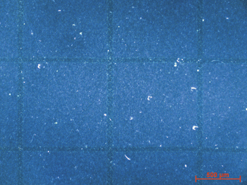
Fig. 6: A macro view of lines created through infrared laser light shows no observable substrate damage.
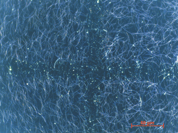
Fig. 7: A micro view of the substrate from Fig. 6 shows no observable features inside the laser-patterned lines.
For comparison purposes, shown are photos of typical laser patterned ITO lines using both conventional bright-field viewing (Fig. 8) and dark-field imaging (Fig. 9). It is useful to note that silver nanowires are invisible when viewed through bright-field microscopes and almost invisible when viewed through dark-field microscopes.
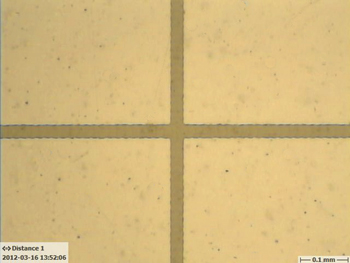
Fig. 8: This bright-field image of laser-patterned ITO clearly shows the lines.
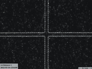
Fig. 9: This dark-field image of laser-patterned ITO shows lines as well.
A Promising Process
High speed laser patterning of silver nanowire is a very promising process. Silver nanowire has shown significant potential in all three major optical areas: light transmission, color, and haze. Since this material is applied using wet coating methods, the equipment cost is typically much less than that of conventional vacuum coating equipment. Further cost savings can be found in the amount of material required, due to the higher conductivity of silver compared to ITO. Moreover, by replacing conventional chemical wet etch with direct laser etch, manufacturers will reduce production costs and eliminate the need for hazardous and expensive chemicals. Most significant is the finding that the use of fiber-based infrared lasers achieves the highest speeds and offers the lowest initial capital cost and long-term maintenance cost of any of the lasers reviewed.
This convergence of technology provides new cost-effective possibilities for the production of touch panels. Laserod has produced an infrared patterning system that can pattern approximately 10,000 parts per day on silver nanowire. Touchscreen manufacturers could scale production capabilities based on the number of machines in use and maintain the flexibility to readily change the pattern designs in a matter of hours. The use of in-house capabilities to apply silver nanowire would add to the flexibility of production and eliminate the need for an oversupply of material and components. Manufacturers could produce products proportionate to market demand, be responsive to new design changes, and potentially generate greater profit.
Acknowledgments
Portions of this article are based on original material from "Wet-Processable Transparent Conductive Materials" by Michael Spaid of Cambrios Technologies, which appeared in the January 2012 issue of Information Display.
Thanks to Cambrios Technologies for providing us with their proprietary silver nanowire (ClearOhm) with which these experiments were conducted. Special thanks to Paul Mansky, Ph.D., of Cambrios for providing invaluable data and analysis assistance. •
Terry Pothoven is Laser Processing Manager with Laserod Technologies. He can be reached at Terry@Laserod.com.