Are MicroLEDs Really the Next Display Revolution?
Are MicroLEDs Really the Next Display Revolution?
Are MicroLEDs Really the Next Display Revolution?
Interest in microLED displays has grown exponentially since the acquisition of microLED maker LuxVue by Apple in 2014. The technology offers the potential for multiple disruptive features, but it is also inherently complex and presents many challenges.
by Eric Virey
TRADITIONALLY packaged, or more recently, chip-scale-package (CSP) light-emitting diodes (LEDs) have been used for more than a decade and are now the omnipresent illumination source in LCD-panel backlights. Various types of packaged LEDs are also used in the large video billboards that are a common sight in stadiums, malls, and video facades (such as in Times Square in Manhattan). In those giant displays, discrete-packaged LEDs containing red, green, and blue chips form the individual pixels, with pitches typically ranging from 1 to 40 mm depending on display size and resolution (Fig. 1).
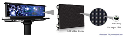
Fig. 1: Traditional LED video walls are based on packaged LEDs. The LED packages used in those applications are black in order to minimize reflection of ambient light and improve contrast.
LEDs, however, have never been used as the direct emissive element (pixel) in small-pitch consumer displays. The reasons for this limitation are multiple and include cost and manufacturability. Nevertheless, the idea of using microLEDs at sub-millimetric pixel pitches to realize a display is almost as old as the invention and commercialization of LEDs themselves.
The concept picked up steam in 2001 after researchers at Kansas State University showed a 10 × 10-pixel-resolution display with 12-µm diameter µLEDs at a 50-µm pitch.1 Various research groups have since been active in the field, including Saitama University,2 Hong Kong University of Science and Technology, ITRI, Sun Yat-Sen University, Columbia University, Tyndall National Institute, University of Illinois, Strathclyde University, CEA-LETI, and many more.
In 2014, excitement in the tech and display communities was palpable after Apple acquired microLED display startup LuxVue. Since then, many large consumer electronics and semiconductor companies have committed to the technology. In 2016, Oculus, the AR/VR arm of social networking behemoth Facebook, first acquired InfiniLED and later licensed patents from mLED, another UK-based microLED startup. In 2017, Sharp acquired eLux, a startup company spun off by its US R&D organization, Sharp Laboratories of America, to develop microLED displays leveraging on the fluidic self-assembly transfer technology the research outfit had been working on since the early 2000s. (The concepts of fluidic self-assembly had been pioneered earlier by Alien Technologies, but Sharp proceeded to develop its own version of the technology independently.)
Later that year, Google invested around $13 million in nanowire LED startup company glō AB (winner, with Jasper Display Company, of an I-Zone honoree award at Display Week 2017), and early this year, Intel led a $35 million funding venture into glō’s competitor Aledia. Finally, Samsung, which had long been rumored to be interested in acquiring Taiwan-based microLED company Playnitride, signed a supply-and-development agreement with leading Chinese LED-chip manufacturer San’an.
Seeing such companies committing to microLEDs shows that whether the technology is being viewed as a sure path toward disruptive displays or more as a defensive project, it is now being taken seriously and is no longer just a lab curiosity.
The Patent Trail
The seriousness is confirmed by looking at patent activity in the sector. A thorough analysis conducted in collaboration with Knowmade, a partner of the author’s company, Yole Développement, shows that more than 120 companies or research organizations have already filed about 1,500 patents in more than 500 families.3 These include startups, display makers, OEMs, semiconductor companies, LED makers, and research institutions. The study also confirms the commitment of companies like Intel and the Chinese company Goertek, which are not typically associated with display technologies. On the flip side, some that are known to be active in the field, e.g. Huawei, have yet to have any published patents in the field.
In any case, as seen in the graph in Fig. 2, patent activity has increased rapidly over the past few years. The patent corpus is relatively young, with an average age of 3.2 years across all families. Sony and Sharp, along with various research institutions, were the first to describe microLED display concepts as early as 2000. Innovative startup companies joined the race in the early 2010s, and display and LED makers are relative latecomers: Most only initiated or ramped up their efforts after Apple showed faith in the technology with the LuxVue acquisition.
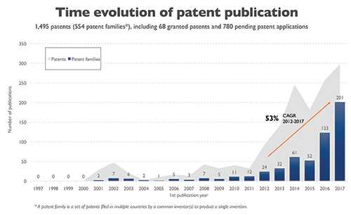
Fig. 2: The number of microLED patent publications has soared, especially from 2012 to 2017. Source: Yole Développement/Knowmade
Tackling a Complex Technology
Complicating matters is that there is no commonly accepted definition for microLEDs. A die with a total surface of less than 2,500 µm2 is generally considered a microLED. This corresponds to a 50 × 50-µm square or a ~55-µm diameter circular die. By this token, it could be argued that microLEDs are already on the market today, unveiled by Sony in 2016 in the form of a small-pitch, large-LED video wall in which packaged LEDs have been replaced by microLEDs about 30 µm in size. But how far off the horizon are small-pitch consumer microLED displays such as those found in our cell phones, smartwatches, TVs, and laptops or in augmented-/mixed-reality head-mounted devices?
To get there, multiple challenges need to be tackled. The art of making microLED displays consists of processing a bulk LED substrate into an array of microLEDs, which are then transferred to a backplane substrate for integration into a heterogeneously integrated system incorporating LEDs, pixel-driving transistors, optics, etc. Epiwafers can accommodate hundreds of millions of µLED chips compared to thousands with traditional LEDs.
There are two major routes to realizing a display from microLEDs. The microchips can be picked up and transferred individually or in groups onto a thin-film transistor (TFT) substrate similar to the ones already used in OLED displays. Alternatively, a full monolithic array of hundreds of thousands of µLEDs can then be hybridized on a CMOS-driving circuit (Fig. 3).
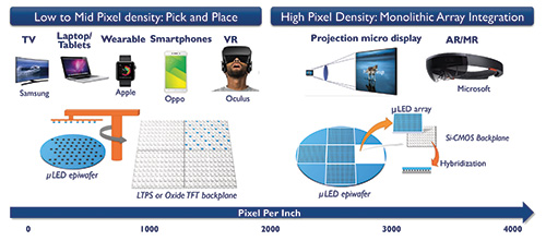
Fig. 3: MicroLED display assembly technologies include pick and place and monolithic array integration. Illustration: Yole Développement
For the former, assembling a 4K display means picking up, positioning, and individually connecting 25 million LED chips (assuming no pixel redundancies) to the transistor backplane. Traditional pick-and-place equipment typically delivers processing speeds of around 25,000 units per hour (UPH). Assuming this equipment could manipulate such small devices, it would take more than one month to assemble a single display! To be cost-compatible with most consumer applications, microLED chip transfer must reach rates of about 50 million to 100 million per hour.
A wide variety of technologies are being investigated to tackle the transfer and assembly challenges. Electromagnetic and electrostatic micro-electro mechanical systems (MEMS) are championed by Apple/LuxVue and others. X-Celeprint got a head start with polymer stamps. Other companies use “sticky tapes,” flexographic and semi-continuous printing processes, or “self-assembly” technologies such as eLux’s fluidic transfer. However, efficient and high-yield transfer of dice below 10 µm remains problematic in most cases.
Another challenge is the LED chip itself. Below 10 µm, microLED operations tend to be dominated by nefarious “sidewall” effects related to surface and subsurface defects such as open bonds, contaminants, or structural damages in which non-radiative carrier recombination dominates. Sidewall effects result from the manufacturing process (plasma etching) and can spread over distances similar to the carrier diffusion length, typically 1 to 10 µm – not a big deal in LEDs that are hundreds of microns large but a killer for microLEDs, where they could affect the entire volume of the chip.
As a result, the reported peak efficiency of microLEDs is often below 10 percent or even 1 percent at the smallest dimensions (<5 µm). This doesn’t compare well with the best traditional “macro” LEDs that now deliver peak external quantum efficiencies above 70 percent.
At low efficiency levels, microLED displays can’t deliver on the key promise of reduced energy consumption. Solving this issue is a key priority. Strategies include new chip designs and improved manufacturing technologies in order to reduce sidewall defects and confine electrical carriers away from the edges of the chip. Other disruptive avenues include nanowire LEDs, which naturally grow 3D structures without sidewall damage.
Other challenging technology nodes include color conversion and light-extraction beam shaping. Interestingly, nobody in the industry seems to agree on what is the most pressing bottleneck. Some see transfer and interconnects as the most daunting challenges; others argue that transfer is just an engineering problem and will soon be solved.
Ultimately, the major issue might be defect management: In modern displays, defective pixels are not acceptable. No matter how good one is at improving epitaxy, chip manufacturing, and assembly yields, defective pixels will always occur. Manufacturers must therefore develop effective defect-management strategies combining pixel redundancies and/or individual pixel repair along with chip and pixel testing and binning. As anticipated, the microLED IP landscape shows a high level of research activity in chip transfer and assembly, but very few solutions have emerged regarding defect management (Fig. 4).
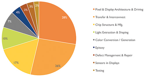
Fig. 4: MicroLED display patents per key technology nodes include pixel and display architecture with 28 percent of the whole, and testing with 2 percent. Source: Yole Développement/Knowmade
Solving the Supply Chain Puzzle
Enabling microLED displays requires bringing together three major areas of expertise: LEDs, TFT or CMOS backplanes, and chip transfer. The supply chain is complex and lengthy compared to that of traditional displays. Each process is critical, and managing every aspect effectively will be challenging. No one company today appears positioned to execute across those multiple technologies and vertically integrate all the components.
Traditional display makers have little experience with LED manufacturing and vice versa. To serve the microLED market, LED makers need to revamp or build greenfield fabs with proper clean rooms and higher resolution lithography. This could be handled by CMOS fabs, which already have depreciated class 10 or 100 clean room, high-resolution steppers, etc. However, LED epitaxy is new to them, so collaboration with LED makers could help jumpstart the supply chain and perhaps even finally establish silicon wafers as a credible microLED platform.
The IP landscape reflects those challenges through the variety of players involved. Only a few companies have a broad microLED IP portfolio, but enough have patents on key technology bricks that complex licensing and legal battles are likely to arise if and when microLED displays enter volume manufacturing (Fig. 5).
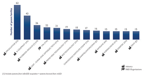
Fig. 5: Top patent assignees are ranked by number of families. Source: Yole Développement/Knowmade
Rolling Out “Real” MicroLED Products
Samsung’s giant 146-in. microLED TV, named “The Wall,” was a major attraction at the 2018 Consumer Electronics Show in Las Vegas (Fig. 6). (“The Wall” is also mentioned in the March/April issue’s Industry News section.) However, despite its 0.84-mm pixel pitch, it doesn’t strictly qualify as “microLED” since it uses traditional SMD-packaged LEDs with chip sizes larger than 0.1 mm. Such displays have been available for some time: Korea-based LED maker Lumens was also showing a 139-in. display with a smaller 0.8-mm pitch at CES, although in a booth of more modest proportions compared to Samsung’s. Some companies such as Leyard-Planar already offer products with even smaller pitches.1
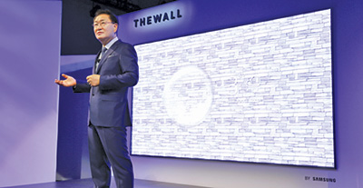
Fig. 6: Samsung’s 146-in. microLED TV was unveiled at the 2018 Consumer Electronics Show.4
Mainstream technology media were quick to tout Samsung’s Wall as the first-ever microLED TV, having obviously forgotten that Sony created a similar buzz back in 2012 when it showed the first microLED TV, a full high-definition 55-in. TV prototype called Crystaled.
At the time of writing, Samsung had yet to release information on pricing for the Wall. The author estimates that each individual LED chip in this display is at least 125 × 250 µm in size. Assuming $600 for the cost of a fully processed 6-in. LED epiwafer, that is about $26,000 for LED chips alone, before singulation, SMD packaging, transfer, assembly, etc. It therefore seems unlikely that such a display could be offered below $250–300K per unit. The Wall is an amazing product for the indoor digital signage market, but it is doubtful that it will trigger riots at your local electronics store on the next Black Friday.
For more than 20 years, the LED industry has delivered impressive cost reductions. There is more ahead, but the low-hanging fruit has already been harvested. To be cost-compatible with the consumer TV market, the LED die must shrink to about 5–10 µm. At this size, the transfer and efficiency challenges are compounded. Smartphones are an even harder nut to crack, with an estimated die-size target of 3 µm or below.
These are aggressive but not unrealistic targets. However, with the current state of technology and factoring in the supply chain challenges, it will probably be at least another three to four years before one could reasonably envision purchasing a microLED TV or smartphone.
Which products come first to market will result from a complex interplay among technology maturity, the evolution of competing technologies such as OLEDs, company strategies, and specific supply-chain requirements for each application.
Yole Développement is optimistic regarding microdisplays to be used in augmented-reality or head-up displays. Many companies and research organizations have already shown convincing prototypes and it is conceivable that a well-funded startup could bring together the different technology bricks and manage the supply chain without having to deploy significant capital expenditure (capex). Once yields are up, major elements such as the LED epiwafer and the CMOS backplane can be outsourced. Those are also applications in which microLEDs are highly differentiating. As a matter of fact, they currently seem to be the only technology capable of delivering the combination of small form factor, low power consumption, and high luminance (hundreds of thousands of nits!) required for those applications.
For high-volume consumer applications such as smartphones or TVs, the cost targets are more aggressive. The high volumes translate into high capex and multiple challenges to set up the supply chain, something that only a large company could enable.
Wearables such as smartwatches fall in between microdisplays and those very high-volume consumer applications. Cost targets enable the use of larger dice and allow pixel redundancy, easing the challenges in defect management. With smaller displays and lower volumes, a motivated company could set up the supply chain through a combination of strategic partnerships and internal investments. As long as the TFT backplane can be outsourced, manufacturing 20 million displays per year for a smartwatch wouldn’t require more than 20 of the latest generation MOCVD multi-wafer reactors and a few dozen transfer tools. This is a lot of money for a startup, but a drop in the bucket for companies like Apple or Samsung. Wearables would be an efficient way to establish a “beta” supply chain and serve as a beachhead before moving on to mid-size displays with high added value such as automotive applications, and finally addressing more challenging applications such as TVs or smartphones.
A Paradigm Shift in TVs
Fifty-five-in. diagonal-size TVs have been commoditized, thanks to the multiplication of Gen-8.5 fabs, which enable efficient production of six panels from a single 5.5 m2 glass substrate. Consumers are now demanding larger 65-in, 75-in., and 85-in. panels, and, although the size of the average living room will eventually limit this trend, many consumers would gladly purchase “wall-sized” TVs up to 110 inches or more if those were affordable. This possibility poses tremendous challenges for TV makers, since the manufacturing of large panels on existing Gen-7, -8, or -8.5 fabs is relatively inefficient (Fig. 7).
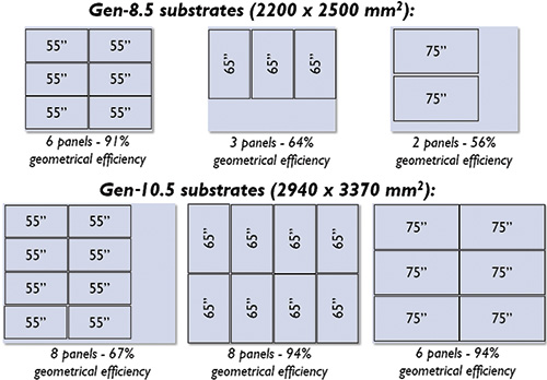
Fig. 7: Panel cuts on Gen-8.5 and Gen-10.5 substrates show different possible configurations. Source: Yole Développement
As a result, prices have remained high. Some panel makers are addressing the challenge by building Generation-10.5 fabs that can efficiently produce 65-in. and 75-in. panels. As of Q1-2018, at least seven of those fabs have been announced and should enter production by 2022, with the first one from BOE coming online as we write. These fabs will help bring costs down, although they come with a pretty stiff price tag, typically around $7 billion, which means significant depreciation costs. (For more about the impact of Gen-10+ fabs, see the article “Gen-10 Fabs Will Create Upheaval in the Display Market” in this issue.) An alternative is to convert mostly depreciated Gen-6, -7.5, or -8.5 fabs to multi-modal glass (MMG) configurations where different sizes of panels are manufactured on the same substrate. However, this also brings added complexity and presupposes that there is a market to absorb the smaller panels.
MicroLEDs offer potentially disruptive answers to this problem as well as ways to create arbitrarily large displays without significant capex.
With traditional displays (LCD, OLED), the cost of both the TFT backplane and the frontplane scales with their area. With microLED, however, the frontplane cost doesn’t scale with the area but with the number of pixels: for a 4K display, the 25-million microLED chips are the same size and cost the same whether they are spread out onto a 55-in. or a 110-in. backplane. Therefore, only the TFT backplane cost scales with the surface.
One could part with the TFT entirely and use discrete silicon chips to drive groups of pixels (Fig. 8). In a 4K 85-in. TV, the pixel pitch is 163 µm. Using 5-µm microLEDs leaves plenty of space for a silicon microchip driver and associated circuitry. These could be assembled by the same technologies used for the microLED. If one assumes that the silicon can drive reasonably large groups of pixels (32 or more), the solution could be to eliminate the traditional TFT backplane entirely. In this case, the cost of a modular TV would essentially be independent of its surface area and would be based instead on the cost of the circuit boards and mechanical assembly. A 110-in. TV would cost essentially the same as a 65-in. unit!
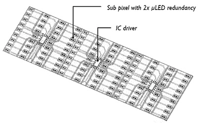
Fig. 8: This µLED display’s discrete ICs positioned on the front face can drive groups of 36 subpixels. This display module features a 2× subpixel redundancy.5
Besides opening the market for very large TVs, this could transform the competitive landscape: This modular construction doesn’t require multibillion-dollar TFT and front-plane fabs. Assembly can be contracted to outsourced semiconductor assembly and test (“OSAT”) companies. This environment could foster new competition in the TV market, where previously, very few companies could absorb the multibillion-dollar fab sticker shock required for suitable expansion.
This rosy scenario of course has its caveat: While the cost of those modular microLED TVs wouldn’t scale with surface size, it would scale with the number of pixels. So expect an 8K TV that requires four times more LED chip and silicon drivers to cost significantly more than a 4K TV. And as the size increases, higher resolution becomes more desirable to maintain the pixel density within the “retinal display” range where individual pixels remain indistinguishable when viewed from a normal distance.
Applications Grow as LEDs Shrink
So how long will we have to wait until we see the first consumer applications? The science is here, but microLED is an inherently complex technology with cost drivers different from those of incumbent materials OLED and LCD. Based on the current status of the developments and the maturity level of the supply chain, late 2019–2020 appears to be the earliest that a product could hit the market. AR microdisplays or wearables are the first candidates. Relatively high-added-value displays such as automotive applications could come next, but large-volume consumer products such as TVs or smartphones will require significantly more time.
There is reasonable expectation that microLEDs will succeed in various segments, but it is still too early in the technology development cycle to assert whether they will take the industry by storm or crash and burn like many other “promising” technologies in the past.
In the meantime, the LED and display industries are already shrinking traditional LED packages or using “chip-on-board” concepts for “miniLEDs.” Those are typically >100 µm in size and don’t present the handling, assembly, and efficiency challenges of microLEDs. MiniLEDs are expected to enter the market by late 2018 in full-array local-dimming (FALD) multizone LCD backlights that could significantly improve black levels, as well as in low-pitch LED videowalls for indoor digital signage.
Finally, the large amount of ongoing research and development on the microLED topic will likely bear fruit and cross-pollinate into other applications, leading to better and more efficient LEDs, high-speed light-fidelity (Li-Fi) communication, lithography applications, and micro-device transfer technologies that could benefit many other industries.
References
1H. X. Jiang et al. “III-Nitride Blue Microdisplays,” Applied Physics Letters 78, 1303, 2001.
2S. Takano et al. “A High Density Full Color LED Display Panel on a Silicon Microreflector,” T. IEE Japan, 121-E, (8), 2001.
3“MicroLED Displays: Intellectual Property Landscape,” Yole Développement, 2018.
4“Samsung Unveils ‘The Wall,’ the World’s First Modular MicroLED 146-inch TV,” news.samsung.com.
5LuxVue patent US 9,318,475: “Flexible display and method of formation with sacrificial release layer.” •
Dr. Eric Virey serves as a senior market and technology analyst at Yole Développement. He holds a Ph.D. in optoelectronics from the National Polytechnic Institute of Grenoble. Virey is a daily contributor to the development of LED, OLED, and display activities, with a large collection of market and technology
reports as well as multiple custom consulting projects. Previously, Virey held various R&D, engineering, manufacturing, and business development positions with Fortune 500 company Saint-Gobain in France and the United States.
This article has been written in collaboration with Dr. Nicolas Baron, CEO of Knowmade and co-author of “MicroLED Displays: Intellectual Property Landscape” (Yole Développement and Knowmade, January 2018).