Amorphous-Metal Thin Films Enable Ultra-High-Definition Display Backplanes
Amorphous-Metal Thin Films Enable Ultra-High-Definition Display Backplanes
Amorphous-metal thin films can enable a new generation of TFT-free display backplanes for ultra-high-definition (UHD) LCD TVs. This technology builds upon previous efforts to commercialize dual-select thin-film-diode backplanes and addresses issues faced by TFTs in UHD-TV applications through use of the amorphous-metal non-linear resistor. Demonstrating the reliability of amorphous-metal-based tunneling electronics and the scalability of these materials to panel-size processing tools are now the key challenges for this technology.
by Sean Muir, Jim Meyer, and John Brewer
THERE is no one-size-fits-all solution for flat-panel-display backplanes. Many backplane technologies exist and each has its pros and cons. To a large extent, choosing a backplane technology depends on the display type and/or application, e.g., liquid crystal or organic light-emitting diode, smart phone or television, home or industrial use, etc.
One area of rapid growth for the display market has been ultra-high-definition (UHD) LCD TVs. Since 2012, the UHD-LCD-TV market has steadily grown from fewer than 100K panels shipped to well over 10 million in 2014.1 Estimates for 2015 UHD-LCD shipments are now at 40 million, indicating that strong growth for this market segment continues.2
The increasing demand for UHD-LCD TVs 50-in. or larger has already put pressure on well-established backplane technologies. Hydrogenated amorphous-silicon (a-Si:H) thin-film-transistor (TFT) UHD-LCD backplanes are fundamentally limited by the low mobility of a-Si:H. Low-temperature polycrystalline silicon (LTPS) TFTs have higher mobility, but their application to UHD-LCD-TV backplanes is hindered by grain-boundary-related large-area uniformity issues, which result in difficulties in scaling to large areas and high-production costs inherent to the use of ion implantation and excimer-laser annealing.
Undesirable attributes associated with a-Si:H and LTPS have stimulated the development of newer technologies such as oxide TFTs for UHD-LCD TVs.3 Oxide TFTs offer improved large-area uniformity compared to LTPS, due to their amorphous structure and higher performance compared to a-Si:H from their increased mobility. However, with these improvements comes an increase in backplane complexity. Oxide TFTs in production typically use an etch-stop-type architecture which requires additional process and photolithography steps.4 These additional process steps can negatively impact production costs and yields.5
The common feature of all of these UHD-TV backplane technologies, as well as of all other (that we are aware of) emerging small- and medium-format backplane technologies, is the use of a TFT. TFT-based backplane performance is primarily defined by TFT channel width (W), length (L), and mobility (µ). Optimizing displays for higher resolution, lower power consumption, and faster refresh rates involves (to a large extent) optimizing TFTs within the “transistor box” defined by W × L × µ. The demands of UHD TV are shrinking the “transistor box” even further as channel W and L must be reduced to maintain decent aperture ratios at higher resolution, i.e., panel light efficiency. However, short-channel effects from this size reduction are significant and can potentially have adverse effects on performance, such as mobility reduction at high gate-source voltages.3
The question as to whether there are alternatives to using TFTs in backplane technology has been asked for some time.6 From the early 1990s to the mid-2000s, metal-insulator-metal thin-film-diode (MIM-TFD) and dual-select-diode (DSD) backplane technologies were developed as low-cost alternatives to TFT backplanes.7–14
The Case for Amorphous Metals
Our team at Amorphyx is developing a new generation of dual-select (DS)
backplanes using amorphous-metal thin films. The device enabling these backplanes is the amorphous-metal non-linear resistor (AMNR). In our discussion, we will first introduce the AMNR device and then describe how it is utilized in an AMNR-DS backplane for UHD LCD TVs. We also present a high-level 2016–2017 roadmap for AMNR technology.
An amorphous-metal thin film generally provides a much smoother surface than that of a normal polycrystalline metal thin film. The reason is simple. An amorphous-metal thin film does not possess grain boundaries. The lack of grain boundaries in an amorphous-metal electrode can smooth out the local work function and enable better control of the electric field in a transistor or a MIM tunneling device.15–18 Figure 1 details a schematic of the atomic arrangement in a crystalline metal compared to that for an amorphous metal, as well as a representative atomic-force micrograph (AFM) for each. Typical amorphous metals can achieve a surface roughness root-mean-square (RMS) of less than 1 nm, whereas typical crystalline metals have an RMS greater (usually much greater) than 1 nm.
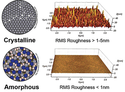
Fig. 1: At left are schematic atomic arrangements of a crystalline metal and an amorphous metal, as well as, at right, a representative atomic-force micrograph for each, highlighting typical differences in surface roughness root-mean-square (RMS).
Introducing the Amorphous-Metal Non-Linear Resistor
The amorphous-metal non-linear resistor (AMNR) is a two-terminal device that employs amorphous-metal thin films to create highly uniform tunnel junctions for regulating current–voltage performance.19 AMNR electrical performance is similar to that of an amorphous-metal-based MIM diode. However, an AMNR exhibits a symmetrical current–voltage curve. This is accomplished through the use of opposing tunnel junctions. Figure 2 shows a cross-sectional view of an AMNR, as well as a top-down view of one possible layout of an AMNR.
As shown in Fig. 2, an AMNR is a three-layered electronic device that can be fabricated using only two photolithography masks. Reduced mask count and process simplicity can potentially have a tremendous impact on device yield and cost. This is precisely why manufacturers invested in MIM-TFD technology throughout the 1990s.7,8 Single-select MIM-TFD technologies struggled with poor gray-scale control and large-area uniformity issues so that they could not compete with a-Si:H TFT backplane technology. The uniformity issues can be solved by moving to a dual-select drive circuit.20 However, the dual-select backplane prototypes produced using SiNx-based MIM-TFDs were leaky in the off-state and only demonstrated 6-bit color resolution.14
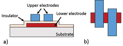
Fig. 2: (a) A cross-sectional schematic of an AMNR device and (b) a top-down view of one possible AMNR layout.
We believe that the availability of an AMNR is a game-changer for dual-select TFD backplane technology. Table 1 highlights how AMNR technology differs from that of previous technology based on a MIM TFD, as well as oxide-TFT backplane technology (using an etch-stop TFT architecture).
Table 1: AMNR, SiNx MIM-TFD, and oxide-TFT technologies are compared in terms of temperature sensitivity, number of lithography steps, and other characteristics and requirements.
| Feature or process step |
AMNR |
MIM-TFD |
Oxide-TFT |
| Conduction Mechanism |
Fowler-Nordheim |
Poole-Frenkel |
Channel |
| Active Material |
Al2O3 |
SiNx |
InGaZnO |
| Light Sensitive |
No |
Yes |
Yes |
| Temperature Sensitivity |
~ –10 mV/K |
~ –30 mV/K |
~ –12–17 mV/K21,22 |
| Lithography Steps (pattern, etch) |
2 |
2 |
5* |
| Sputter Depositions (metals, oxide) |
2 |
2 |
3 |
| PECVD Depositions (Insulators, passivation, etch stops) |
1 |
1 |
3* |
| Total Thickness |
<200 nm |
>400 nm |
>500 nm |
| Registration Tolerance |
>5 µm |
>5 µm |
1-2 µm |
*For an etch-stop TFT architecture.
Amorphous-metal lower electrodes allow for thin high-K dielectrics, such as Al2O3, to be used as a tunneling insulator in an AMNR, while maintaining low leakage current in the off-state. The use of a thick SiNx dielectric for previous-generation dual-select backplanes led to Poole–Frenkel trap-assisted emission as the dominant conduction mechanism. Poole–Frenkel emission is difficult to control since it depends on the nature and
density of traps present in the insulator. Also, Poole–Frenkel emission leads to I–V curves that are non-abrupt and temperature-dependent. In contrast, use of a thin Al2O3 insulator leads to electron conduction via Fowler–Nordheim tunneling in an AMNR.
An AMNR is an electronic device without a semiconductor. This is an important point. In fact, it is hard to overemphasize its importance. Since an AMNR is a semiconductor-free device that employs Fowler–Nordheim tunneling as its operative mechanism, an AMNR has low temperature and light sensitivity compared to that of Poole–Frenkel or channel-conduction-dependent devices. Fowler–Nordheim tunneling yields I–V curves that are abrupt and nearly temperature independent. Fowler–Nordheim tunneling is the mechanism used in flash memory. By utilizing Fowler–Nordheim conduction, the leakage current of an AMNR is reduced, leading to less shift of the subpixel data voltage between each frame refresh and the potential to eliminate subpixel storage capacitors. Figures 3(a)–3(f) show example I–V curves for an AMNR, a SiNx-based non-linear resistor used in prior-generation dual-select backplanes10 and a typical metal-oxide IGZO-TFT.23
Figures 3(a)–3(c) highlight a key difference between AMNRs and other technologies. The AMNR is not as leaky as a SiNx-based device. Compared to a SiNx device, the AMNR conducts much less in the low-field region. Additionally, it has a more abrupt turn-on.
The AMNR is bi-directional. Bi-directionality allows the select voltage for an AMNR-based subpixel to be either negative or positive. However, the use of a bi-directional current has implications for AMNR device reliability. By changing the polarity of the select voltage with each subpixel activation, the AMNR experiences a symmetrical voltage waveform. Use of a symmetrical voltage waveform improves threshold-voltage stability and device reliability.
The AMNR does not conduct at 0 V. Since it does not conduct at 0 V, the AMNR does not need to be negatively biased to transition to a fully off-state unlike most TFTs.
Figures 3(d)–3(f) demonstrate that the AMNR has a wide operating range. It can operate at elevated temperatures and under direct illumination with only a minor shift of its I–V curve. One way to shift the threshold voltage of an AMNR is simply to change the thickness of its insulator; however, this will also alter the dominant conduction mechanism. If the insulator is too thin, device operation is dominated by direct tunneling with a high leakage current. If the insulator is too thick, phonon-assisted tunneling or another more complicated and thermally activated conduction mechanism becomes operative. To maintain Fowler–Nordheim conduction as the dominant mechanism, while increasing the threshold voltage, the number of AMNR tunnel junctions can be increased. This allows for a more flexible design in which both low- and high-operating voltage Fowler–Nordheim- based AMNRs are used, as shown in Fig. 3(f).
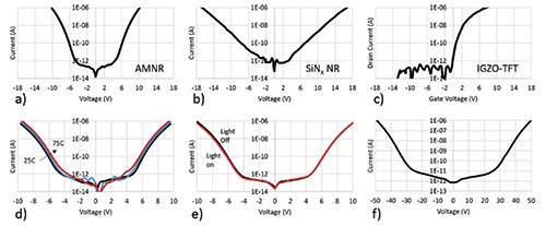
Fig. 3: (a) Examples of room I–V curves are shown for an AMNR, (b) a SiNx-based non-linear resistor, (c) an IGZO-based TFT, (d) an AMNR at elevated temperatures, (e) an AMNR under illumination, and (f) a high-field AMNR. The SiNx non-linear resistor curve is adapted from Ref. 10, whereas the IGZO-TFT curve is adapted from Ref. 23.
Using the AMNR in a Dual-Select Backplane
As the name implies, a dual-select backplane requires the use of two select lines in addition to a data voltage line. A typical TFT backplane for a LCD has one select line and one data line. Circuit schematics for a dual-select subpixel and for a typical 1-TFT 1-capacitor (1T1C) liquid-crystal subpixel are shown in Figs 4(a) and 4(b).20
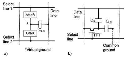
Fig. 4: Circuit schematics for (a) a dual-select AMNR subpixel and (b) a typical 1T-1C subpixel. The schematics are adapted from Ref 20.
A key difference between the dual-select TFD circuit and the 1T1C circuit is that the liquid-crystal capacitor (CLC) for each subpixel is not tied to a common ground. The dual-select circuit is driven differentially, essentially creating a virtual ground for each subpixel when the two AMNRs become activated. The data voltage for each subpixel is set relative to this virtual ground during the AMNR “on” period. The use of a differential circuit effectively cancels out AMNR variations across the display area and over time. The cancellation provided by this configuration makes the AMNR-DS backplane well-suited to large-area-display applications.
Early dual-select display prototypes produced using SiNx-based non-linear resistors showed crosstalk between subpixels due to the large capacitance of these devices. To eliminate crosstalk, the offset, scan, and hold (OSH) drive scheme was developed.9,11 Figure 5 shows schematic select and data voltage waveforms for the standard and OHS dual-select drive schemes.
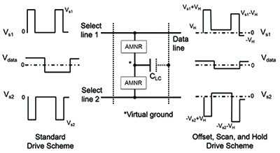
Fig. 5: Schematic select and data voltage waveforms for the standard and OSH dual-select drive schemes are shown left and right, respectively. Drive scheme waveforms adapted from Ref. 9.
The OSH drive scheme puts the virtual ground at a non-zero but sub-threshold “offset” value between frame refresh cycles. This reduces the total voltage swing on CLC between data voltage inversions, allowing for the use of 5-V data drivers and thereby reducing the voltage that the AMNR experiences in the off-state. The OSH drive scheme therefore reduces the sensitivity of the data voltage to AMNR leakage current non-uniformities and improves high-temperature operation.
The low leakage current of the AMNR combined with the use of an OSH drive scheme can eliminate the need for a storage capacitor. Furthermore, an AMNR for an UHD LCD has a small footprint, estimated at 1–5% of the total subpixel area for 50–100-in.-diagonal displays with UHD (4K) and FUHD (8K) pixel densities. Because of the compact nature of the AMNR and its ability to eliminate the need for a storage capacitor, AMNR backplanes for UHD and FUHD are expected to provide aperture ratios in excess of 50%, despite the need for an additional AMNR select line.
The Future for AMNR Backplane Technology
To firmly establish the AMNR as a backplane contender, future AMNR technology development will be focused on reliability, scalability, and flexibility, as
shown in Fig. 6.
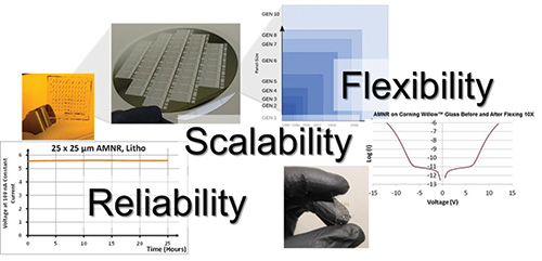
Fig. 6: The future development of the AMNR is focused on three main areas: reliability, scalability, and flexibility. The lower left insert shows a reliability stress-test plot for a “champion” AMNR device that did not fail after 24 hours of continuous stress at 100 nA. The upper insets depict how the AMNR has already been scaled from 1- to 6-in. substrates and is now being scaled to Gen 2.5 “prototype” sizes. The lower right insets show a Corning Willow glass substrate with AMNR devices being flexed as well as I–V plots for an AMNR device before and after flexing of its substrate.
Reliability
Accelerated lifetime testing of AMNR devices at 100% duty cycle has shown “champion” devices that last well beyond 50,000 hours at a 100-nA current when scaled to high-resolution duty cycles (e.g., UHD = 0.046% duty cycle, so that 24 hours @100% equals 52,174 hours @ 0.046%). While these results are very encouraging, a complete display-backplane package requires the availability of appropriate models for predicting AMNR performance and reliability. AMNR studies involving variable stress, temperature, duty cycle, frequency, and storage conditions are all under way in order to formulate robust physically based models. The techniques available for evaluating the performance and reliability of thin-gate dielectrics for transistors are generally identical to those needed to evaluate AMNR performance. AMNR reliability analysis therefore draws on the same standards used for transistor reliability analysis, such as the JEDEC (Joint Electron Device
Engineering Council) standards, JESD35-A, and JESD92.24–26
Scalability
AMNR research and development is now focused on the use of 6-in. wafers. Each wafer contains a large number of test devices for statistical process control assessment, as well as a wide variety of devices to facilitate process optimization. The exercise of scaling from a 1-in. substrate toolset to a 6-in. toolset has revealed that amorphous-metal thin-film quality can vary from toolset to toolset, as one might expect. However, once basic differences in configuration, environmental baselines, and sputter conditions have been taken into account, it is possible to port AMNR technology from one toolset (and location) to another. AMNR technology assessment is now transitioning to a Gen 2.5 prototype line.
Flexibility
Flexible backplanes are another application in which AMNR technology is a possible game-changer. Amorphous metals are flexible. For example, amorphous-metal thin films have been commercialized as hinges for digital micromirror devices.27 An AMNR is thin. As shown in Table 1, the total thickness of a typical AMNR is less than 200 nm. Use of a thinner layer tends to reduce film stress, thereby leading to a backplane device that is more robust and flexible. An AMNR offers wide registration tolerance. AMNR performance is defined by the total tunneling area and insulator thickness, not by channel dimensions, as in a TFT. Thus, AMNR registration tolerance can be 3× or more than that of a TFT, as shown in Table 1. Wide registration tolerance make an AMNR well suited to roll-to-roll processing, which has the potential to completely redefine backplane manufacturing
processes and cost structures. The flexibility of an amorphous metal and the thinness and wide process registration tolerance of an AMNR bode well for the use of AMNRs in future flexible-display products.
AMNR technology is now being commercialized through the Amorphyx AMNR Consortium. This technology consortium is similar to those created to accelerate the
development of flexible electronics or OLED technologies.28–30 The key focus of the AMNR Consortium is to address critical device and panel level issues so that members are better positioned to translate AMNR technology into production. Amorphyx has partnered with the Industrial Technology Research Institute in Taiwan to host the AMNR Consortium beginning in 2016. High-level goals for the AMNR Consortium include (1) verifying reliability and scalability, (2) developing device models, drive schemes, and subpixel layouts to maximize display performance, and (3) building prototype AMNR-based displays to evaluate crosstalk and subpixel bit resolution.
Acknowledgment
AMNR research and development has been funded in part through a National Science Foundation Small Business Innovative Research grant (#1345460 and #1456411).
References
1IHS: 4K TV Panel Shipments Reached a Monthly Record of 3 Million Units in April 2015, IHS Says | IHS Online Newsroom at <http://press.ihs.com/press-release/design-supply-chain-media/4k-tv-panel-shipments-reached-monthly-record-3-million-units>
2IHS: UHD LCD TV Panels to Exceed 40% of Total Shipment Area in 2016, IHS Says | IHS Online Newsroom at <http://press.ihs.com/press-release/technology/uhd-lcd-tv-panels-exceed-40-percent-total-shipment-area-2016-ihs-says>
3S. C. Kim, Y. S. Kim, E. K-H. Yu, and J. Kanicki, “Short channel amorphous In–Ga–Zn–O thin-film transistor arrays for ultra-high definition active matrix liquid crystal displays: Electrical properties and stability,” Solid-State Electron. 111, 67–75 (2015).
4P. Singer, “Applied Materials rolls out new CVD and PVD systems for IGZO-based displays,” Solid State Technology (2013) at <http://semimd.com/blog/2013/10/17/applied-materials-rolls-out-new-cvd-and-pvd-systems-for-igzo-based-displays/>
5D. Hsieh, “How 4K x 2K LCD TVs affect display panel manufacturing yields,” DisplaySearch Monitor (2012) at <http://electroiq.com/blog/2012/07/how-4k-2k-lcd-tvs-affect-display-panel-manufacturing-yields/>
6W. den Boer et al., “Are There Alternatives to TFTs in AMLCDs?” Information Display 10, 2–5 (2006).
7K. Takahashi et al., “A high image-quality LCD addressed by lateral MIM,” Proc. International Display Research Conference 247–250 (1991).
8S. Kamagami, K. Sunohara, Y. Tanaka, and H. Morita, “Display performance improvement in a TFD-LCD with reduced image-sticking,” Proc. International Display Research Conference, 199–202 (1991).
9W. den Boer, M. Boyd, and V. Veerasamy, “Elimination of Cross-talk in Dual-MIM-LCDs,” Proceedings of the International Display Workshops (1998).
10W. den Boer et al., “Dual Branch MIM Array Technology for Low-Cost AMLCDs,” SID Digest of Tech Papers, 1–4 (1998).
11W. den Boer, “A Select Line Driver for the Offset-Scan-and-Hold Dual Select Diode AMLCDs,” SID Digest of Tech Papers, 44–47 (2001).
12W. den Boer and G. S. Smith, “Dual select diode AMLCDs: A path towards scalable two-mask array designs,” J. Soc. Info. Display 13, 199 (2005).
13W. den Boer and G. S. Smith, “Recent Progress in Low Cost Dual-Select-Diode AMLCD Technology,” Proc. IMID, 873–877 (2005).
14W. den Boer et al., “Low Cost Dual-Select-Diode AMLCD Technology,” SID Digest of Tech Papers (2006).
15K. Ohmori et al., “Impact of additional factors in threshold voltage variability of metal/high-k gate stacks and its reduction by controlling crystalline structure and grain size in the metal gates,” Proc. IEEE International Electron Devices Meeting, 1–4 (2008).
16M. E. Grubbs, X. Zhang, M. Deal, Y. Nishi, and B. M. Clemens, “Development and characterization of high temperature stable Ta-W-Si-C amorphous
metal gates,” Appl. Phys. Lett. 97, 223505–223505–3 (2010).
17E. Cowell III, et al. “Advancing MIM Electronics: Amorphous Metal Electrodes,” Adv. Mater. 23, 74–78 (2011).
18T. Matsukawa et al., “Impact of granular work function variation in a gate electrode on low-frequency noise for fin field-effect transistors,” Appl. Phys. Express 8, 044201 (2015).
19W. E. Cowell III, “Amorphous metal thin-film non-linear resistor,” WO2014074360 A1. (2014).
20W. den Boer, Active Matrix Liquid Crystal Displays: Fundamentals and Applications (Elsevier, The Netherlands, 2005).
21C. Chen, K. Abe, H. Kumomi, and J. Kanicki, “Density of States of a-InGaZnO from Temperature-Dependent Field-Effect Studies,” IEEE Trans. Electron Devices 56, 1177–1183 (2009).
22S. C. Kim, Y. S. Kim, and J. Kanicki, “Density of states of short channel amorphous In–Ga–Zn–O thin-film transistor arrays fabricated using manufacturable processes,” Jpn. J. Appl. Phys. 54.
23T.-Y. Hsieh, T.-C. Chang, T.-C. Chen, and M-Y. Tsai, “Review of Present Reliability Challenges in Amorphous In-Ga-Zn-O Thin Film Transistors,”ECS J. Solid State Sci. Technol. 3, Q3058–Q3070 (2014).
24J. S. Suehle, “Reproducibility of JEDEC Standard Current and Voltage Ramp Test Procedures for Thin-Dielectric Breakdown Characterization,” Integrated Reliability Workshop Final Report, 22–34 (1993).
25“Procedure for Wafer Level Testing of Thin Dielectrics,” JESD35-A (2001).
26“Procedure for Characterizing Time-Dependent Dielectric Beakdown of Ultra-Thin Gate Dielectrics,” JESD92 (2003).
27J. Tregilgas, “How We Developed an Amorphous Hinge Material,” Adv. Mater. Process. 163, 46–49 (2005).
28FlexTech | Alliance for Displays & flexible, printed Electronics. at <http://flextech.org/>
29Merck KGaA Leads OLED Consortium | Latest News | Chemical & Engineering News at <https://pubs.acs.org/cen/news/87/i45/8745news3.html>
30Sony Global–INCJ, JDI, Sony, and Panasonic announce the establishment of JOLED, Inc. A new integrated company in organic
light-emitting diode display panels at <http://www.sony.net/SonyInfo/News/Press/201407/14-0731E/> •
Sean Muir is the Vice-President of Device Technology, Jim Meyer is Director of Technology Transfer, and John Brewer is CEO/President of Amorphyx. They can be reached at smuir@amorphyx.com, jmeyer@amorphyx.com, and jbrewer@amorphyx.com, respectively.