Industry News November/December 2013 Issue 6
Technicolor Offers Color and 4K Certification Programs
The Technicolor process for color motion pictures was invented in 1916. Since then, the process and the companies behind it have changed considerably, but Technicolor is still synonymous with state-of-the-art Hollywood technology.
In a program designed to leverage that cachet, Technicolor began partnering with color calibration software company Portrait Displays last year to provide a color certification program for PCs and mobile devices. More recently, Technicolor also began offering 4K image certification for 2K to 4K image conversion (rather than to actual devices), supplying its first Image Certification to Marseille Networks for its system-on-a-chip designed to deliver 4K TV content.
Technicolor’s color specification is based on software from Portrait Displays, which is designed to be used by OEMs to fine tune screens for color accuracy. The result should be consistent color across all certified devices. The colors seen in movies watched on certified laptops, tablets, and smartphones will match exactly those intended by the creators of the movies. The certification will also extend to online shopping – so you don’t buy a yellow sweater online thinking it is green, for example – and to videos and photos taken by consumers. Licensed OEMS will be able to offer the certification logos on their products (Fig. 1).
Both the color and 4K device-certification programs were announced some time ago (the color one in 2012 and the 4K one last summer), but rollout has only recently begun, with the Toshiba BDX4600 Blu-ray player receiving 4K image certification.
Fig. 1: These logos will appear on color-certified devices.
Lighting Exhibition Features OLEDs and LEDs
A unique exhibition under way in Germany right now features lighting technologies based on LEDs, OLEDs, and other materials. In addition to demos of state-of-the-art lighting design, including walk-in installations (Fig. 2), the “Lightopia” exhibition includes a mock laboratory (Fig. 3) designed to explain the science behind LEDs and OLEDs. The show also examines the historical role that lighting has played in shaping human environments, including its environmental ramifications. Lightopia is taking place at the Vitra Design Museum in Weil am Rhein (Germany) through March 16, 2014. The exhibition is sponsored in part by Merck, which developed many of the materials used in the exhibits.
“Innovative lighting offers new application possibilities, which require close collaboration between designers and manufacturers,” says Jolanthe Kugler, curator of the exhibition. After its run at the Vitra Design Museum, Lightopia will go on tour to other museums throughout the world.
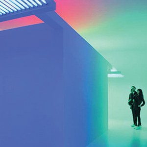
Fig. 2: The Lightopia exhibition at the Vitra Design Museum features walk-in installations such as this fluorescent-based work by artist Carlos Cruz-Diez. Image courtesy © Carlos Cruz-DieIz & Adagp, Paris 2013.
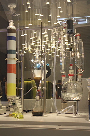
Fig. 3: Merck contributed a mock laboratory exhibit to Lightopia that was designed to explain how LEDs and OLEDs are made. Image courtesy Merck.
Samsung/Cheil Industries to Acquire Novaled
Samsung Electronics and Samsung affiliate Cheil Industries have signed an agreement to acquire OLED technologies and materials provider Novaled in a transaction valuing Novaled at €260 million
According to a press release from Novaled,1 Cheil Industries, a leading display materials supplier, will acquire a majority stake of approximately 50% in Novaled. Samsung Electronics will acquire approximately 40%. The remaining stake of approximately 10% is currently held by Samsung Venture Investment, which will maintain its current shareholding. The transaction includes a €30 million contingent payment, which is conditional on reaching certain milestones.
Most industry experts say the acquisition is clearly designed to bolster Samsung’s OLED expertise, making it more competitive in developing large OLED TVs for the mass market, for example. Cheil Industries’ CEO Jong-Woo Park had this to say in Novaled’s press release: “Leadership in [the] future display market will be determined by technological capacity,” and “this acquisition is expected to generate significant synergy in new-generation OLED materials R&D and will play a critical role in enhancing Cheil Industries’ market position as a global leader in electronic materials.”
1http://www.novaled.com/press_news/news_press_releases/newsitem/cheil_industries_to_acquire_novaled_ag/
Apple Announces New Products before the Holidays
As Information Display was going to press, Apple announced new iPads and computers, as well as a free version of the OS X upgrade Mavericks. A thinner, lighter version of the company’s larger (9.7-in.) tablet, named the iPad Air, was scheduled to go on sale Nov. 1, at prices starting at $499. A new iPad mini with a Retina display (2048 × 1536) and a more powerful processor (A7) than previous versions was slated for availability later in November for $399. The company also announced an updated line of Retina MacBook Pros and a new Mac Pro desktop in what is perhaps the company’s most minimalist design yet – a small black cylinder.
New Deposition Systems Target Metal-Oxide TFTs
Applied Materials, a manufacturer of systems for the semiconductor, flat-panel display, and solar photovoltaic industries, recently announced new deposition systems for manufacturing large-sized and ultra-high-definition LC and OLED displays. The Applied Materials AKT-PiVot 55K DT PVD, Applied AKT-PiVot 25K DT PVD, and Applied AKT 55KS PECVD systems are designed to work with metal-oxide films to manufacture smaller, faster thin-film transistors required to create high-resolution displays.
Metal-oxide-based TFTs enable low-power high-resolution smart phones and tablets as well as some OLED TV technologies. Future 4K TVs are also expected to use metal-oxide TFTs. However, this technology has proved challenging in terms of uniformity and scale in mass production. The uniformity and particle control of Applied Material’s PVD and CVD systems is designed to help realize the newest display technologies with high yield in mass production.
Applied Materials’s AKT-PiVot DT PVD systems (55K for 2200 mm × 2500 mm and 25K for 1500 mm × 1850 mm substrates) use the company’s proprietary rotary cathode array technology to deliver uniform, homogeneous, and low-defect active-layer deposition for metal oxide as well as interconnect metals and pixel electrodes (Fig. 4).
Applied Material’s new AKT 55KS PECVD system brings precision PECVD technology to 2200 mm × 2500 mm size substrates. The system deposits a dielectric-layer interface for metal-oxide transistors with a new advanced-quality silicon oxide (SiO2) process that minimizes hydrogen impurities to improve long-term transistor stability and optimize screen performance.
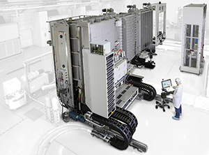
Fig. 4: Applied Materials’ new AKT-PiVot DT PVD system is designed for metal-oxide deposition for large-sized panels (up to Gen 8.5).
2013 Marks 125th Anniversary of Liquid Crystals
Last September, at a scientific forum hosted by the German Chemical Society in Darmstadt, Germany, liquid-crystal-manufacturer Merck helped mark the 125th anniversary of the discovery of liquid crystals. Key properties of cholesteric liquid crystals were discovered by Austrian scientist Friedrich Reinitzer and German physicist Otto Lehmann in 1888.
A highlight of the forum was Merck’s exhibition featuring items dating back to those original discoveries, as well as future-oriented developments such as a smart window in which liquid crystals are used to modify the light transmission properties of the glass.
This year also marked the passing of LCD pioneer Rudolf Eidenschink, who performed groundbreaking research in liquid crystals at Merck for many years. Eidenschink received SID’s Karl Ferdinand Braun Prize in 2011. His obituary can be found in the In Memoriam section of Information Display online.
– Jenny Donelan