New Polymer Materials Enable a Variety of Flexible Substrates
New Polymer Materials Enable a Variety of Flexible Substrates
New Polymer Materials Enable a Variety of Flexible Substrates
The Pylux family of polysulfide thermosetting polymers (PSTs) has been developed to enhance manufacturing options for a wide range of flexible displays and electronics.
by Tolis Voutsas, Radu Reit, Adrian Avendano, David Arreaga, and John Dupree
THE flat-panel display industry has made a remarkable journey since its beginnings in the early 1980s. Continuous improvements in materials, processes, and device technologies have rapidly transformed clunky, power-hungry, and inelegant early displays to thin, high-resolution, brilliant, and aesthetically pleasing panels that have completely transformed the way we communicate and interact.1,2 All this has been accomplished with the same fundamental form factor, consisting of an essentially rigid display surface. Overcoming this constraint has been the focus of intense R&D work, almost since the very first days of flat panels, to enable new and innovative flexible form factors.3,4 According to the 2016 IHS Market Tracker, the market for flexible displays is expected to grow to $26 billion by 2023.5
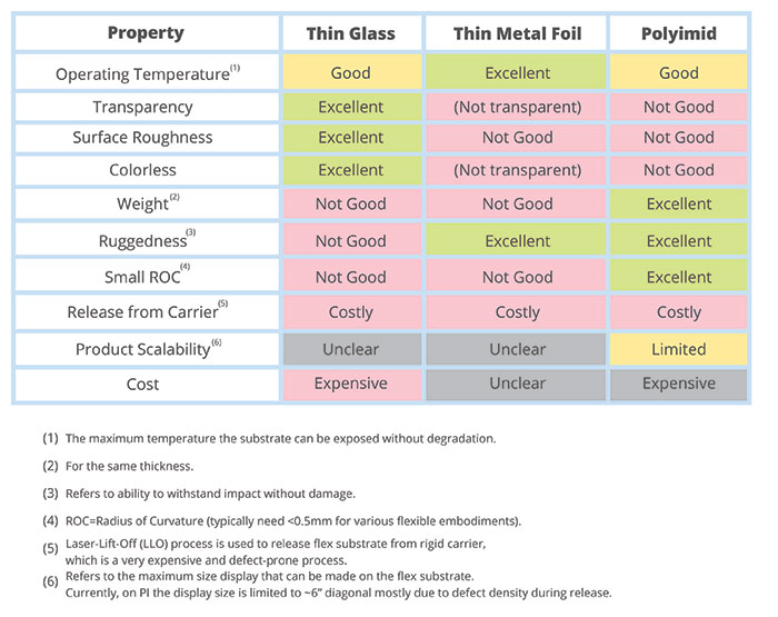
The most stubborn technical challenge of making a flexible display has been finding a suitable substrate material. Beyond the obvious requirement of being flexible, the substrate must satisfy a combination of several, often conflicting, physical properties while at the same time allowing ease of manufacturing and low cost to display fabricators. Over the years, different types of flexible substrates have been developed and evaluated, including inorganic materials (thin metal foil,6 thin glass7,8) and organic materials (polyimide or PI9
). In terms of organic materials, polyimide has become, by default, the current industry standard, primarily due to its operating temperature range and the sheer amount of research that has been done to fit it into pilot manufacturing.
The comparison in Table 1 of various flexible substrates that have been adapted to flexible display
manufacturing indicates that there is no one ideal substrate option, even though substrate materials themselves represent a lucrative $1 to $2 billion market. Substrates are still dominated by outdated materials, some of which date back to the 1930s and 1950s. Part of the problem is that incumbent providers are large, entrenched, and not incentivized to innovate, since innovation would cannibalize their existing market. They are therefore committed to incremental changes within existing technology platforms. The result is a gap between what existing material systems can deliver and what the display industry needs to create new product categories.
Table 1: Comparison of substrate materials for flexible displays
To help close this gap, the authors’ company developed the Pylux family of polysulfide thermosetting polymers (PSTs). The PST family is the culmination of more than 10 years of research at the University of Texas at Dallas, initially around novel materials for neural interfaces. These devices, which intimately contact the central and peripheral nervous system, undergo many of the same stringent thermal and chemical processes as displays during their photolithographic definition (e.g., high-temperature PECVD for SiNx encapsulation layers, wet-etch protocols, lift-off processing, etc.). After successfully building devices for neural interface applications, the team discovered that those materials had applications beyond biomedical implants, not the least of which was offering substrate options to the global display industry. The development and commercialization of PSTs for the flexible electronics space provided the impetus around which the company, Ares Materials, was founded in 2014.
PST Characteristics
PSTs have been formulated precisely for the needs of the flexible electronics industry. The polymer resin can be die-coated or spin-casted at the target thickness and then cured to form a solid film. Its formulation process does not use solvents, which provides for significant cost savings for display manufacturers in terms of process time (less curing time), and raw materials costs. Lack of solvents also translates to a safer and greener process. The resulting solid film is colorless, with high optical transmission (>90% in 450-nm to 800-nm range) and an extremely smooth surface (<0.5-nm surface roughness). This low surface roughness is another key advantage, as it eliminates the need for a surface planarization layer prior to microfabrication of electronic devices and circuits. Figure 1 compares the fabrication process for PST and PI film.
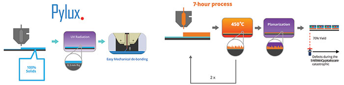
Fig. 1: The preparation process for Pylux is shown at left, and that for polyimide substrates is shown at right.
PST films not only have much lower cure stress than polyimide, but the development of special release layers allows for easy detachment of the film from the underlying carrier using only a mechanical process. This has two distinct advantages over other methods: It eliminates the need for laser-liftoff (LLO), which is a capital-intensive and relatively slow process, and it significantly improves release yield by reducing the occurrence of potentially catastrophic defects during the release process. As a result, both manufacturing cost and manufactured product size can be significantly improved.
Polyimide substrates are solution cast from precursor poly(amic acid) solutions, wherein solvated poly(amic acid) is coated onto the mother glass carrier and baked to remove the high solvent fraction (> 80%). Next, further baking of the dried poly(amic acid) is carefully performed under inert atmospheres to imidize the film and set the final polyimide film. In contrast, PST resin is dispensed onto the mother glass carrier using similar coating techniques (e.g., slot-die coating), where the zero-solvent system can convert the wet film completely to a dry film. Additionally, the material can be converted to the final film in an ambient environment via ultraviolet curing or thermal curing at temperatures below 250°C. PST films show excellent thermal stability up to temperatures of 300°C, with no evolved sulfur species that may interact with subsequent thin-film
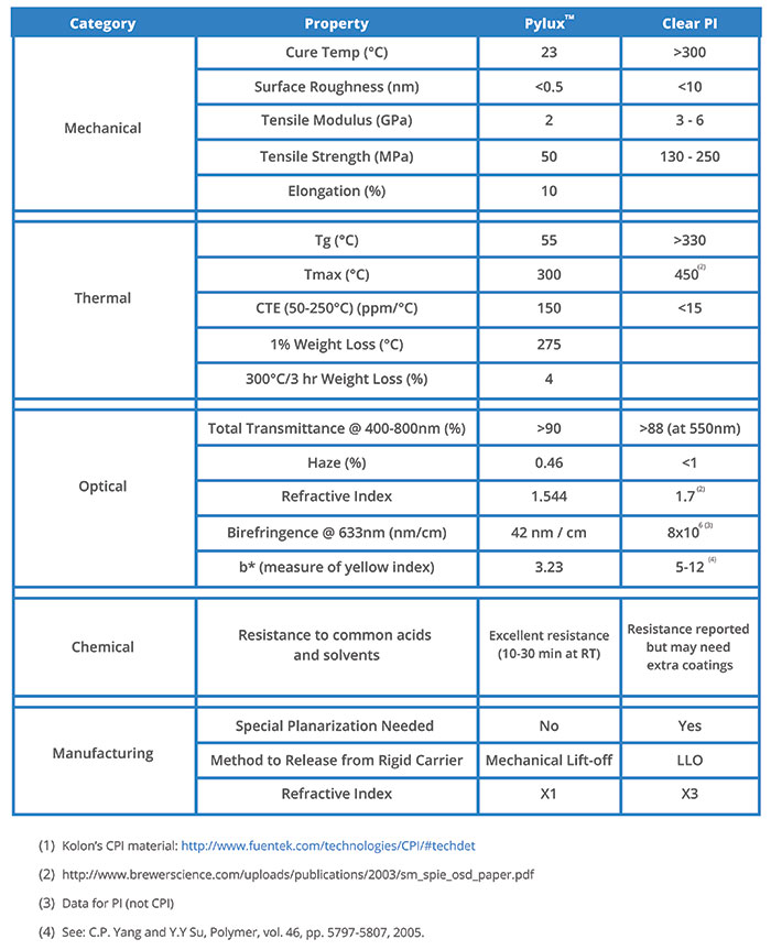
layers. Processes for both Pylux and PI are diagrammed in Fig. 1. Table 2 summarizes various key properties for PST films. Since most flexible substrates in use today are made from clear polyimide (CPI), CPI-equivalent parameters have been included when available.10 It is important to note that PST’s glass transition (Tg) and co-efficient of thermal expansion (CTE) are quite different from the equivalent parameters for typical display-grade polymers. While PST films have a higher Tg and CTE compared to currently used substrates for flexible electronics, these parameters actually comprise the principle used to allow PST to introduce lower stresses related to thermal-cycling thin films deposited atop it. The primary mechanism behind this stress reduction is related to both the lowered Young’s modulus (E) of PST throughout the entire deposition temperature range and to the Tg that further reduces the modulus another two orders of magnitude at the low temperature of 55°C.
Table 2: Pylux and clear PI are compared in terms of key properties1
Often-cited examples for understanding thin-film stresses that accumulate in multi-layer structures include the original Stoney formula for bi-material strips, as well as the countless modifications and expansions of this initial formula.11–17 In these calculations, the total stress observed by a thin-film (σf) for two substrates of equal dimensions reduces to a direct proportionality between the thin-film stress and the Young’s modulus of the substrate (σf ∝ Es). As shown in Fig. 2(a), this is reflected by the low Tg and lowered glassy E of PST. Effectively, this translates to a lowered buildup of thermal stress in the thin films deposited atop the substrate material [Fig. 2(b)], where despite the higher thermal stress-ramp rate close to Tg for PST, the transition from glass to rubber allows for a more attenuated thermal-stress buildup at temperatures subsequent to the Tg. While this is only a brief overview of the mechanics under which the PST operates to
accommodate mechanical mismatch with a variety of thin-film materials, the explanation serves as a good starting point for exploring the use of alternative substrates for flexible electronics.
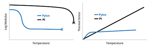
Fig. 2: (a) A log-linear example plots Young’s modulus vs. temperature for Pylux and general polyimides, with thermal
degradation temperatures represented by Xs. (b) Total thermal stress in thin films deposited atop each substrate is shown as a function of temperature.
Figure 3 summarizes the operating temperature range for PST and several other types of
polymer substrates. Despite its lower maximum temperature (e.g., as compared to PI/CPI), PST is the only material that shows no observable mechanical mismatch over its full operating temperature range. The lower maximum temperature that PST can be exposed to (~300°C) vs. that of PI/CPI (~400–450°C) means that it is not suitable for current LTPS-TFT processes. However, current industry trends point toward the eventual adoption of oxide-TFT processes to reduce array manufacturing costs. Since oxide-TFT fabrication can be accomplished at a temperature range that is compatible with PST,18–21 PST will not only be a very desirable substrate option for oxide-based flexible displays, but its very availability should spur market evolution to oxide TFTs. Moreover, the combination of superior dimensional stability, low stress, and excellent adhesion also provide a compelling case for the penetration of PST into the emerging area of OTFT (organic TFT)-based flexible arrays.22 The data in Table 2 also highlight the excellent optical characteristics of PST beyond transparency, such as low haze, very low birefringence, and low yellow index. These reveal another host of front-plane applications for PST that are difficult (or impossible) to access by competing material solutions (e.g., CPI) due to inferior characteristics and/or high cost. Figure 3 shows critical temperature details for various polymer substrate materials.
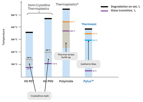
Fig. 3: Critical temperatures for various polymer substrate materials are compared.
Examples of PST Applications
Figure 4 summarizes some of the possible applications of PST material in LCD and OLED stacks. Based on its combined optical, mechanical, and thermal properties, PST will be able to provide material solutions for the TFT substrate, color filter substrate, touch sensor substrate, cover lens, and OCA. Currently, Ares is working with various partners to test and optimize the PST material for these applications. We have already fabricated IGZO-TFT on PST and compared its performance to that of control devices on silicon substrates (Fig. 5). The thin-film transistors were fabricated on PST at a maximum processing temperature of 250°C. Mobilities of IGZO transistors (W = 100 um; L = 40 um) on PST substrates were an average of 9.1 cm2/Vs, compared to 9.5 cm2/Vs for those directly on Si wafers. Similar on-voltages (–0.2 V vs. –0.6 V) and subthreshold swings (280 mV/dec vs. 293 mV/dec) were also observed when comparing transistor sets on PST substrates vs. those on silicon. The close similarity between the performance characteristics of devices fabricated on PST and those of IGZO-TFTs fabricated on Si carrier wafers validates the compatibility of PST with standard IGZO fabrication facilities and process flow. Using our proprietary mechanical release method and release layer, we were able to ensure that the IGZO-TFT characteristics remained stable even after the release of the PST substrate from the rigid carrier.
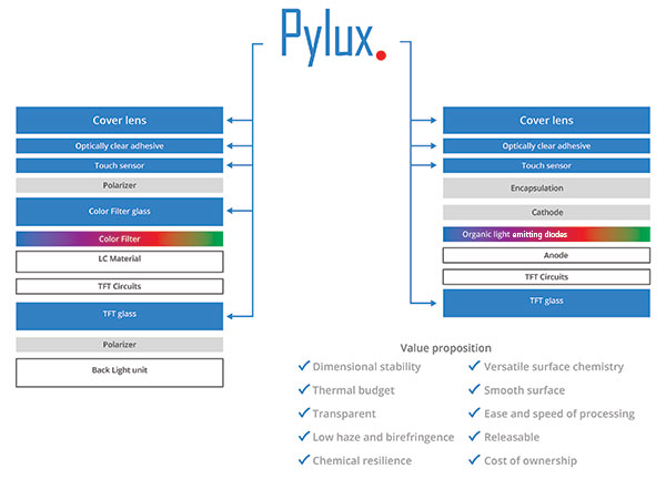
Fig. 4: Potential PST applications for both AMLCD and AMOLED display stacks are indicated with arrows.
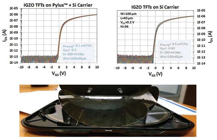
Fig. 5: At top left are I-V curves for IGZO-TFTs on PST formed on a rigid Si carrier. At top right are I-V curves for IGZO-TFTs on a rigid Si carrier. At bottom is a 100-um PST with IGZO-TFTs after release from a rigid Si carrier.
Although PST was originally formulated for sheet-to-sheet processing, Ares has also been developing roll-to-roll capabilities. Recent work done in collaboration with a third party provides evidence that PST is capable of rapid photo-curing (<10 s) and can be implemented in a web configuration. We are also engineering the basic polymer material to exhibit an increased Tg, which eliminates the need for support liners during web processing. This opens up further applications in the broader space of flexible and printed electronics.
PST Materials Are Poised for a Variety of New Applications
The display industry requires new flexible substrate materials with superior optical, mechanical, chemical, and thermal properties that can provide solutions for various display layers, including the TFT substrate, color filter substrate, touch sensor substrate, cover lens, and OCA. Our PST materials have been formulated with these properties, with expected commercial pricing of net realized material that falls below the current range for high-performance PIs. The PST can be die-coated or spin-casted at the target thickness and then
UV-cured to form a solid film. We have already developed a mature sheet-to-sheet process for this material and are in on-going development for a qualified roll-to-roll process.
The company is currently working with over a dozen partners around the world to test and optimize our material for the display and non-display applications noted above. We are completing larger display testing (Gen 2 or larger), and have also successfully achieved our first 10x scale increase in the polymer production process, with additional production scale leaps anticipated for later this year. Commercial production is scheduled to commence by the end of 2017.
Note
Pylux refers to the PST family of polymer materials and is a registered trademark of Ares Materials, Inc.
References
1M. Kubo, et al., “Flexible High-Resolution Full-Color Top-Emitting Active-Matrix Organic Light Emitting Diode Display,” JSID 21, 422–432, 2013.
2Y. Yamamoto and A.T. Voutsas, “Technology Trend of AMLCDs for Mobile Application,” Electrochem. Soc. Transactions 3, 11–22, 2006.
3A. Chida, et al., “Flexible High-Resolution Full-Color Top-Emitting Active-Matrix Organic Light Emitting Diode Display,” JSID 21, 422–432, 2013.
4R. Komatsu, et al., “Repeatedly Foldable AMOLED Display,” JSID 23, 41–49, 2015.
5IHS Flexible Display Market Tracker – H2, 2016.
6T.-K. Chuang, et al., “Polysilicon TFT Technology on Flexible Metal-Foil for AMPLED Displays,” JSID 15, 455–461, 2007.
7www.corning.com/worldwide/en/innovation/corning-emerging-innovations/corning-willow-glass.html
8www.agc.com/english/products/products_07.html
9S. Nakano, et al., “Highly Reliable a-IGZO TFT on a Plastic Substrate for Flexible AMOLED Displays,” JSID 20, 493–498, 2012.
10www.fuentek.com/technologies/CPI/#techdet
11G. G. Stoney, “The Tension of Metallic Films Deposited by Electrolysis,” Math. Phys. Character 82(553) 172–175, 1909.
12S. Timoshenko, “Analysis of Bi-Metal Thermostats,” J. Opt. Soc. Am. 11(3), 233, 1925.
13Y. Inoue and Y. Kobatake, “Mechanics of adhesive joints – Part III. Evaluation of residual stresses,” Appl. Sci. Res. Sect. A 7(4), 314–324, 1958.
14R. Glang, R. A. Holmwood, and R. L. Rosenfeld, “Determination of Stress in Films on Single Crystalline Silicon Substrates,” Rev. Sci. Instrum. 36(1), 7–10, 1965.
15C. Atkinson and R. V. Craster, “Theoretical aspects of fracture mechanics,” Prog. Aerosp. Sci. 31(1), 1–83, 1995.
16K. Röll, “Analysis of stress and strain distribution in thin films and substrates,” J. Appl. Phys. 47(7), 3224–3229, 1976.
17M. Yanaka, Y. Tsukahara, N. Nakaso, and N. Takeda, “Cracking phenomena of brittle films in nanostructure composites analysed by a
modified shear lag model with residual strain,” J. Mater. Sci. 33(8), 2111–2119, 1998.
18J. Lee, et al., “World’s Largest (15-inch) XGA AMLCD Panel Using IGZO Oxide TFT,” SID Symp. Digest of Tech. Papers, 2008.
19K. Miura, et al., “Low-Temperature-Processed IGZO TFTs for Flexible AMOLED with Integrated Gate Driver Circuits,” SID Symp. Digest of Tech. Papers, 2011.
20D. Geng, H. M. Kim, M. Mativenga, Y. F. Chen, and J. Jang, “High Resolution Flexible AMOLED with Integrated Gate-Driver using Bulk-Accumulation a-IGZO TFTs,” SID Symp. Digest of Tech. Papers, 2015.
21H. J. Kim, “Various Low-Temperature Activation Methods for IGZO TFTs in Flexible Displays,” SID Symp. Digest of Tech. Papers, 2016.
22C. W. M. Harrison, et al., “Flexible AMOLED Display Driven by Organic TFTs on a Plastic Substrate,” SID Symp. Digest of Tech. Papers, 2014. •
Tolis Voutsas, Radu Reit, Adrian Avendano, David Arreaga, and John Dupree are with Ares Materials, Inc. Voutsas can be reached at tolis@aresmaterials.com.