Lasers Enable Diverse Display Production Techniques
Laser-based techniques are finding increased use in certain aspects of flat-panel-display manufacturing. Lasers provide the option of a non-contact high-spatial-resolution tool that is appropriate for a variety of processing tasks, including thin-glass cutting, laser direct patterning, low-temperature-polysilicon annealing, and laser lift-off.
by Rainer Paetzel
DISPLAY MANUFACTURERS continually face market pressure to improve display performance and reduce product weight and thickness without significantly increasing cost. Several innovative manufacturing technologies have been developed to address the resultant fabrication challenges, and the laser has emerged as a critical enabling tool for many of them. This article reviews four major laser-based techniques currently being employed in display production: thin-glass cutting, laser direct patterning, low-temperature polysilicon annealing, and laser lift-off for flexible-display manufacture.
Thin-Glass Cutting
The conventional mechanical technique for cutting glass has certain drawbacks for very thin substrates, such as those used in miniature displays. In particular, the mechanical force of the cutting tool produces microcracks in the material, and the subsequent breaking step yields small chips and debris, plus an edge that is not necessarily perpendicular to the glass surface. Furthermore, mechanical cutting leaves significant stress in the finished edge. To prevent further cracking or breaking in downstream handling and processing, it may therefore be necessary to grind or polish the cut surface after cutting. Also, a post-process cleaning step may be required to remove debris that could otherwise interfere with subsequent processes, such as circuit formation.
Laser glass cutting is a non-contact process that eliminates the problems of microcracking and chipping. Also, laser cutting produces essentially no residual stress in the glass, result-ing in higher edge strength. This is critical because even when force is applied to the center of a glass panel, any break usually initiates at the edge. Consequently, laser-cut glass can withstand two to three times as much force as mechanically cut glass.
Laser cutting can also reduce the number of process steps, since it does not require any subsequent cleaning or grinding stages. Therefore, while the capital cost for a laser-cutting station is higher than for a mechani-cal system, the overall investment in laser cutting can be lower than for mechanical processing if an additional grinding machinecan be eliminated. As a result of the above factors, laser processing has been widely adopted in the display industry for the cut-ting of glass substrates having a thickness of1 mm or less because this is the area where the technology's advantages are most pro-nounced. In terms of processing speed, some laser glass-cutting techniques are faster than their mechanical counterparts; some are slower (see Table 1 below for a comparison).
Table 1: Comparison of mechanical and laser glass-cutting methods
| |
Mechanical Scribe
|
Laser Scribe
|
Laser Full-Body Cut
|
| Speed* |
500 mm/sec
|
<1500 mm/sec
|
<20 mm/sec
|
| Accuracy |
50 μm
|
25 μm>
|
200 μm
|
| Thickness range |
30 μm – 20 mm
|
200 μm – 10 mm
|
30 μm – 1 mm
|
| Cooling |
—
|
Water, ethanol, CO2
|
Clean dry air, nitrogen
|
| Post processing |
Breaking, grinding, cleaning
|
Breaking
|
—
|
*Based on 0.5-mm-thick sodalime glass, with a 200-W laser and water cooling.
There are two basic laser-based techniques for glass cutting: laser scribing, which is primarily used for substrates in the 0.3–0.7-mm thickness range and laser full-body cutting, which is utilized mostly with very thin substrates of 0.2 mm or less. Both methods typically use a continuous-wave (CW) CO2 laser or a pulsed CO2 laser with a repetition rate high enough to appear as a CW at the feed rates used in this application.
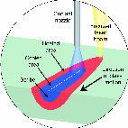
In laser scribing, the laser is focused onto the surface of the glass, which is translated so as to create a continuous cut. Since all glasses strongly absorb the 10.6-μm CO2 laser wavelength, all the laser energy is deposited at or near the surface of the glass, causing rapid heating. Either liquid or air is then delivered by nozzles onto the glass to quickly cool it; the resulting thermal shock produces a continuous crack in the glass that is typically about 100 μm deep (Fig. 1). After the entire scribing is com-pleted, the glass then passes under a mechanical roller or controlled chopper bar that imparts enough force to propagate the crack through the entire substrate and break it. This break is free of debris and perpendicular to the surface.
Laser full-body cutting utilizes an alternative, non-mechanical method for breaking the glass. Here, the original scribe crack is created by a laser beam but with cooling only from an air or nitrogen jet. A second laser beam then causes rapid expansion of the glass and drives the crack all the way through the substrate, eliminating the need for a separate breaking process. No cooling is used with the second laser beam.
The set-up for laser full-body cutting is similar to that of laser scribing, with translation of the substrate. The table summarizes the characteristics of mechanical cutting and the two laser techniques.
Laser Direct Patterning
Lithography is used to pattern circuit elements at various production stages for several different display technologies. Conventionally, the photolithographic process involves at least six separate steps (resist coating, baking, exposure, developing, etching, and resist stripping). Each of these steps requires dedicated capital equipment, which takes up manufacturing floor space and each requires time to complete. Additionally, some of these processes involve chemicals that are not environmentally friendly.
In some cases, a single step in which a laser directly ablates a material layer can replace the six steps of conventional lithography. Laser direct patterning can increase manufacturing efficiency by reducing cycle time, increasing yields, and reducing manufacturing floor space, as well as decreasing the environmental impact of production.
Currently, a common application for laser direct patterning is in selectively removing the clear conductive layer of indium tin oxide (ITO) on the front glass of a plasma-display panel (PDP) to form the front electrodes. This task is usually performed using a multimode Nd:YAG operating in the near-infrared.
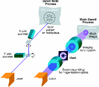
Most laser-based micromachining is performed using either a direct-write or a mask-based approach (see Fig. 2). In the case of ITO patterning, a combination of the two processes is employed. In particular, a mask is used to define the pattern and the laser is raster-scanned over the large glass substrate, rather than illuminating it all at once. This process produces the desired pattern on the work surface. The multimode Nd:YAG laser is the machine of choice for this application as long as relatively low resolution is required; this is because it is inexpensive, yet still supplies sufficient optical power to enable the process to occur at adequate throughput rates. Estimates are that about half of the PDPs currently in production are laser processed in this manner.
 Coherent GmbH
Fig. 1: Laser scribing creates a continuous crack through the glass.
 Coherent GmbH
Fig. 2: Direct-write and mask-based laser processes are shown side by side. In direct writing, the focused laser beam is scanned by galvanometer mirrors to trace out the desired pattern on the workpiece; in mask-based imaging, the laser illuminates a mask containing the desired pattern, which is then re-imaged on the workpiece.
The laser-generated features on PDPs are several hundreds of microns in size. However, there are other applications in the production of other FPD types that require higher resolution. For example, in some LCD architectures, the transparent-conducting-oxide (TCO) electrodes on the color-filter panel must be precisely formed in order to properly shape the electrical field, which controls the vertical alignment of the liquid-crystal molecules within each red, green, and blue subpixel. The feature sizes of these electrodes are on the order of 5 μm and below; i.e., too small to be patterned by Nd:YAG lasers. These are currently produced lithographically.
The only practical laser method to achieve the spatial resolution and placement accuracy necessary for this task is to use an excimer laser in a mask-imaging process. This application is currently at an early stage of development and has not been deployed in production by any manufacturer. The deep ultra-violet output of the excimer laser enables production of micron-sized and even sub-micron-sized features (which is why they are used for integrated-circuit microlithography). In addition, the high pulse energy of the excimer laser can remove the entire TCO thin film in a single pulse, thus providing the required process throughput rate. The mask pattern is imaged at a demagnification on the work surface. This makes the power density on the mask much lower than that achieved on the work surface (see Fig. 2). To make this process practical, a mask must be created containing the circuit pattern for a large number of pixels to enable the parallel ablation of many pixels with one laser pulse. After each exposure is made, the substrate must then be translated relative to the laser beam for another shot; this is repeated until the entire display is processed.
Another emerging laser process is producing scribe lines on touch screens. Specifically, touch-screen production usually involves scribing multiple lines of about 25–50 μm in width through a TCO layer. The laser-based process for touch-screen scribing uses a high-power diode-pumped solid-state laser operating in the ultraviolet (typically over 20 W at 355 nm). Once again, the short UV wavelength can easily be focused to produce the desired feature size. Furthermore, this wavelength does not penetrate far into the substrate, meaning a minimal heat load on what is often a delicate thin glass or plastic substrate. The physical size of the scribe patterns, together with their simplicity (usually a checkerboard configuration), can be easily produced with a direct-write process.
Low-Temperature-Polysilicon Annealing
In active FPDs, silicon forms the basic semi-conductive layer for the build-up of the thin-film transistors (TFTs) of the active matrix for various display applications including LCDs. This layer is initially created by standard PE- or LP-CVD techniques and is amorphous in nature. Amorphous silicon (a-Si) is the dominant material used in FPDs today; however, it has limited electron mobility, which in turn drives compromises in other aspects of display designs. Increasing the electron mobility is highly desirable and electron mobility can be dramatically increased by converting the a-Si into polysilicon (poly-Si) through an annealing (re-crystallization) process.
Increasing electron mobility delivers several benefits. First, it enables the implementation of smaller TFTs supporting higher aperture ratios and therefore brighter AMLCDs and/or higher overall electrical efficiency. Smaller TFTs can also enable higher-resolution displays. It also makes it practical to implement drivers and other circuitry directly on the display, simplifying overall system construction and lowering total costs. As a result, poly-Si annealing is a critical enabler for system-on-panel (SoP/SoG) displays. It also delivers the ideal combination of high performance and reliability to act as an ideal support matrix for AMOLEDs. However, despite the performance benefits of poly-Si, its use is unlikely to spread beyond these display types any time soon.
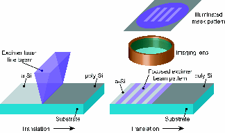
Excimer-laser-based low-temperature-polysilicon (LTPS) annealing is now the preferred approach for producing the poly-Si layer during FPD fabrication because it can be performed at low temperatures, possibly as low as 200°C. At present, the two LTPS techniques most widely used are excimer-laser annealing (ELA) and sequential lateral solidification (SLS). Both of these require excimer lasers that combine high pulse energy (1 J) and repetition rates of several hundred hertz at very high-energy stability (Fig. 3).
 Coherent GmbH
Fig. 3: Shown is the ELA polysilicon annealing processes (left) and the SLS process (right). In ELA, the excimer beam is shaped into a long line and scanned over the substrate. In SLS, the laser beam is projected as a series of stripes onto the substrate. An exposure is made and then the substrate is translated by half the pitch of the pattern for another exposure.
In ELA, the rectangular beam from a 308-nm excimer laser is optically homo-genized and re-shaped to form a long narrow line (typically around 465 mm x 0.4 mm) that has a high degree of energy uniformity throughout its profile. This line profile is directed at the silicon-coated substrate, which is then scanned relative to the beam.
Silicon efficiently absorbs 308-nm radiation, making it possible to achieve near-complete melt with each individual pulse. This leads to effi-cient crystal formation due to crystal growth in the vertical direction, starting at the interface between the molten and residual unmolten silicon.
In SLS, the laser beam is projected through a mask, creating a striped pattern on the substrate. This particular mask design makes it possible to scan the substrate and crystallize each location by just two consecutive laser pulses. The first pulse melts through the entire depth of the Si layer, producing a pattern of lines of poly-Si with a-Si in between. The typical line width is a few microns. The substrate is then offset by half the line pitch of the mask for the next exposure. This exactly fills in the area missed in the first exposure, yielding a continuous layer of laterally crystallized polysilicon.
The primary advantage of SLS is that it can potentially deliver as much as twice the throughput over ELA for the same process requirements. However, at the present time, the industry uses ELA almost exclusively, and it is the only process qualified for mass production of AMOLEDs.
Laser Lift-Off
Flexible displays have enormous commercial potential, but their introduction has been slowed by several significant technical challenges. In particular, the thin plastics substrates used for flexible displays are too delicate to be handled with conventional tooling and will typically lose their limited rigidity at the high temperatures experienced in some production steps. Thus, flexible-display production requires either substantial process modification or will be restricted to a very small range of materials.
Two laser techniques – SUFTLA (surface-free technology by laser annealing) and EPLAR (electronics on plastic by laser release) – have already proven capable of avoiding these limitations. Both techniques employ the same concept to enable mass production of flexible displays – fabricating the display circuitry on a rigid substrate using conventional methods and then using the laser to deposit highly localized energy at a layer or interface, allowing lift-off of the active devices from the rigid carrier.
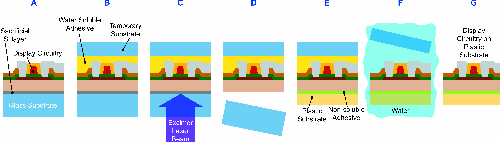
In SUFTLA, a sacrificial silicon layer is deposited on a standard substrate, and display circuitry is fabricated on top of this layer using completely conventional methods. Then, a series of steps are performed to bond the circuitry to a temporary substrate, release the original glass substrate, and then bond to a permanent, flexible plastic substrate (see Fig. 4). This technique was developed by Seiko-Epson and is currently used in products based on E Ink technology.
Electronics on plastic by laser release is another lift-off process, pioneered by Philips Research and is currently being used in production. Here, a polyimide film is spun onto the glass substrate prior to device fabrication. The polyimide is baked to a temperature higher than any used for subsequent TFT processing steps. Once again, display circuitry is fabricated using completely conventional methods. The plastic can withstand this processing because it is physically supported by the glass substrate. Next, a high-power ultraviolet excimer laser is directed through the glass substrate. This light is absorbed strongly by the plastic and a thin layer of it is ablated, thus separating the flexible display from the carrier.
Both SUFTLA and EPLAR offer similar benefits. Specifically, they employ rigid glass carriers, thus eliminating the need for special handling during fabrication, and they allow the use of standard processes and tools for display circuitry fabrication. Additionally, the glass substrates can be cleaned and reused repeatedly.
In conclusion, lasers are finding increasing use in FPD manufacture. They offer a non-contact high-spatial-resolution tool that is useful for a variety of processing and measurement tasks. In many instances, these characteristics result in increased yields, higher throughput, improved performance, and more environmentally friendly production. •
 Coherent GmbH
Fig. 4: SUFTLA process overview: (a) Display circuitry is fabricated over a sacrificial layer on a glass substrate. (b) The circuitry is bonded to a temporary substrate. (c) The laser ablates the sacrificial layer. (d) The circuitry separates from the glass substrate. (e) The flexible plastic substrate is permanently bonded to the circuitry. (f) Water dissolves the adhesive holding the temporary substrate. (g) The display is now on a flexible substrate.
Rainer Paetzel is Director of Marketing for Coherent (Deutschland) GmbH, Dieselstraße 5 b , D-64807, Dieburg, Germany; telephone +49-551-6938155, e-mail: rainer.paetzel@ coherent.com. Coherent GmbH is a maker of lasers, laser-based systems, precision optics, and related accessories.