Transparent Film and Substrate Technology for Touch Screens and Flexible-Display Applications
Flexible electronic displays with touch screens are increasingly used in demanding outdoor environments. Design engineers are challenged to develop optical systems that meet a wide thermal range (–40° to +85°C) and comply with diverse optical, electrical, and mechanical parameters. This article describes possible solutions, including transparent thin-film anti-reflective and conductive coatings. Also discussed are technologies being currently employed such as conductive transparent oxides [e.g., indium tin oxide (ITO)], carbon nanotubes, and silver nano-particles. The optical and mechanical properties of substrates used in the fabrication of flexible displays and touch screens are also reviewed.
by Jeff Blake and Richard Paynton
A great deal of interest surrounds the use of flexible displays with touch screens for a variety of commercial, industrial, and military applications. A June 2010 Display Bank report1 estimated that the market for flexible displays will exceed $2.4 billion in 2015 and $30 billion by 2020. Their attractiveness over rigid, glass displays/substrates is based on their attributes such as lighter weight, thinner profile, potential lower manufacturing costs, and their ability to be incorporated into a wide variety of products. Applications being investigated and developed for flexible technology include wrist-mounted displays, electronic books and paper, cell phones, and tablet computers. An "unbreakable" display that provides good optical properties, requires low power, and is cost-effective would certainly be in great demand. Technology applicable to flexible displays is already being used in the manufacture of photovoltaics, RFID tags, solid-state lighting (OLEDs), touch screens, and, most recently, transparent displays.
As appealing as this technology is, display and touch-screen design engineers now face significant technical challenges in the development and manufacture of flexible-display systems, including:
• Display and touch-screen format: The flexural modulus must be defined for use in product fabrication and functionality. In order to have a complete user-interface system, both the display and touch screen must be flexible and compatible.
• Display technology and material processing: As described in Table 1, material limitations exist in the development of transmissive (e.g., LCDs), reflective (e.g., cholesteric displays), and emissive (e.g., OLEDs) materials for use in flexible-display applications.
• Substrates: Plastic films, flexible glass, or metal backplanes: Limitations include gas permeability, lower processing temperatures, and mechanical durability for plastic films; impact resistance and flexibility for glass; and transparency and surface roughness for metal foil.
• Touch-screen technology: Resistive touch screens require physical contact of the conductive layers for activation. At the same time, separation needs to be maintained between the top and bottom films while they are not in use. If the touch screen is flexed, it could generate a false activation or signal distortion as well as sensitivity variations.
• Coatings: ITO, the most common transparent conductive material used in resistive and capacitive touch screens and many displays, will crack when flexed to too small of a radius. Promising nano-materials such as graphene or carbon-nanotube (CNT) coatings are just becoming widely available for commercial applications and should offer alternatives as technologies mature. Alternative conductive materials (CNTs and silver nano-particles) are generally more flexible than ITO and can be readily patterned. Current market-barrier issues that are being addressed include cost, transparency, and sheet resistance.
Table 1: Material limitations exist in the development of transmissive, reflective, and emissive materials for use in flexible-display applications
| Material or Process |
Use in Display or Touch Screen |
Limitations or Issues |
| Substrate: flexible glass |
Front surface cover of flexible display or touch screen |
Can break, limited flexibility, may be difficult to process R2R |
| Substrate: PET (polyethylene terephthalate) |
Front surface of flexible display or front and rear surface of a touch screen |
Requires high-performance gas-barrier coatings to prevent damage of displays (e.g., OLEDs), relatively low processing temperature may limit some manufacturing processes to be used, birefringent |
| Substrate: PEN (polyethylene napthalate) |
Front and rear surface of flexible touch screens and liquid-crystal encapsulant in flexible displays |
Requires high-performance gas-barrier coatings to prevent the damage of displays (e.g., OLEDs), relatively low processing temperature may limit some manufacturing processes to be used, birefringent |
| ITO coatings |
Transparent conductive coatings used in the production of flexible displays and touch screens |
Brittleness of ITO may limit use in some flexible display applications |
| Graphene & CNT coatings |
ITO replacement materials used as a transparent conductive layer in displays and touch screens |
Transmission, resistance, cost and availability may limit near term applications |
To address these issues, a variety of new materials, optical coatings, films, and manufacturing processes are necessary to aid in the development of flexible displays and improve the mechanical durability and functionality of flexible-display/touch-screen systems. Designers must have a complete understanding of the construction, properties, and interaction of various materials used to manufacture flexible touch screens and displays. These include current common flexible substrates such as PET (polyethylene terephthalate) and PEN (polyethylene naphthalate), barrier films, transparent conductive coatings such as ITO, graphene coatings, and silver nano-particle and CNT coatings.
Assessing Flexibility
In order to select the appropriate materials, the engineering design approach must consider the necessary degree of material flexibility and mechanical, optical, and electrical properties. Authors such as Fihn and Ekkaia2 have developed a hierarchy of display and touch-screen flexibility as follows:
1. Rollable: The display or touch screen can be completely rolled (360°) repeatedly without being damaged.
2. Bendable: The edges of the display or touch screen can meet repeatedly without damage.
3. Semi-flexible: The screen can deflect at least 45° many times without damage.
4. Mostly rigid: The screen can deflect somewhat, but may sustain damage if bent too far or too often.
5. Rigid: Use of some flexible materials; however, damage most likely will occur if screen is flexed.
6. Completely rigid: The screen uses all rigid materials, such as glass that cannot be flexed without damage.
The primary types of flexible displays are shown in Table 2. There are many variations of these types of displays under development at universities, government labs, and R&D centers worldwide.
Table 2: Different underlying technologies for flexible displays all come with advantages and disadvantages.
| Display Type |
Description |
Attributes |
Limitations |
Commercialization Stage |
| Liquid-Crystal Display (transmissive) |
Full-color high-resolution displays using novel flexible materials |
Good resolution, luminance, and contrast. Can be equipped with touch sensor for user interface. |
Requires substitution of transparent plastic materials for glass LC encapsulation |
Demonstrated technology (e.g.,Toshiba, Fujitsu) |
| Liquid-Crystal Display (reflective) |
Medium-color high-resolution displays using novel flexible materials |
Good resolution and contrast. Can be equipped with touch sensor for user interface. |
Requires substitution of plastic materials for LC encapsulation and can be made with metal backplanes |
Demonstrated technology |
| Electrophoretic |
Typically monochrome electronic paper-type display |
Low cost, fairly developed technology. Generally used PET films. |
Requires low-temperature processing. Technology has been demonstrated with plastic and metal backplanes. |
In commercial production (e.g., E Ink, AUO) |
| Organic Light-Emitting Diodes |
Color emissive (does not require backlights). AMOLED and OLED technology has been demonstrated. |
Very good color saturation and viewing angle |
Flexible materials used need to have very low oxygen and water permeability. Plastic films require complex transparent high-performance gas-barrier coatings. |
Demonstrated on low-rate production scale with PEN and PI films (e.g., Sony, Samsung) |
| Cholesteric |
Low-power, monochrome, or full-color (using three colored layers) graphical. Uses bistable, cholesteric liquid crystals. |
Low cost does not require polarizers or backlights; is being produced in R2R process; can be activated with electrical current or pressure |
Is not high resolution, which limits applications and has slow response times. Limits applications that require high refresh rates (e.g., video). |
In commercial production (e.g.,Kent Displays) |
| Light-Emitting Diodes |
Individual LEDs are applied to flexible substrates (e.g., PET) |
Can be very bright |
Not high resolution |
Demonstrated on small scale |
Most commonly, the rigid glass used in typical LCD touch-screen displays is replaced with lightweight, transparent, flexible films such as polycarbonate, acrylic, polyethylene naphthalate (PEN), or polyethylene terephthalate (PET). As shown in Table 3, the trade-offs for using flexible films instead of glass include less optical transparency, lower processing temperature (due to plastic film's higher coefficient of thermal expansion, which causes potential distortion and lower glass-transition temperature), and high oxygen and water permeability (which, in the case of OLEDs, will quickly destroy the display). The advantages of using flexible substrates include lighter weight, increased impact resistance, and lower material and processing costs when produced with high-speed roll-to-roll (R2R) processes.
Table 3: The trade-offs for using flexible films instead of glass include lower optical transparency, lower processing temperature, high permeability to oxygen and moisture, and softer substrate surfaces.
| Substrate |
Visible-Light Transmission (VLT) (380–780 nm) |
Glass Transition Temperature (Tg) in °C |
Water-Vapor Transmission Rate at 38°C, ASTM E-96 Procedure E |
Gas Permeability of Oxygen |
Coefficient of Thermal Expansion (cm/cm x 10-5/°C) |
Refractive Index @ 589 nm |
| Polyethylene terephthalate (PET)* |
85–88% |
150 |
>100 (12 mil thickness) to >2,200 (1 mil thickness) cc/100 in.2/24 hours |
>2 (0°C ) to >12 (50°C ) cc/100 in.2/atm/mil |
4.32 |
1.64–1.67 |
| Borosilicate glass** |
91.7% |
557 |
— |
— |
0.72 |
1.52 |
*DuPont Mylar polyester film
**Schott North America D 263 glass.
The obvious advantage of higher throughput R2R processing is somewhat offset by the required lower processing temperature and the potential for inducing stress into the films during processing. Common deposition processes used to deposit dielectrics and semiconductor materials (e.g., silicon oxide or silicon nitride) in the production of flexible displays include plasma-enhanced chemical vapor deposition (PECVD) as well as printed, gravure, or spray coating. Process selection, in addition to material throughput, is typically dictated by the thermal stability, moisture, and oxygen performance of the organic and in-organic materials being deposited. In addition, printed electronics require very accurate registration (sometimes as accurate as 1 μm) of materials deposited and removed via photo-lithography. Due to the relatively high co-efficients of thermal expansion (CTE) of plastic films such as PET and PEN, the processing temperature must be controlled in order to minimize the delamination of deposited materials as well as the proper registration of printed circuits and coatings.
Transparent Thin-Film Conductive Coatings
In flexible-display manufacturing, organic materials are often deposited in a wet chemical process (e.g., sol-gel condensation) at atmospheric pressures in a combination of a vacuum or sputtering deposition of inorganic conductive metals or metallic oxides. The addition of post-processing films to improve the optical, mechanical, or electrical performance of flexible displays includes adding anti-glare or anti-reflective front-surface films, conductive films, or conductive grids for electromagnetic interference/radio-frequency interference (EMI/RFI) shielding. In the case of resistive or capacitive touch screens, a patterned conductive coating or grid provides the location of the XY coordinates in touch-sensor activation.
Key parameters in selecting transparent conductive coatings include photopic transmission, absorption, and reflection in addition to coating resistance, durability, and cost.
Transparent thin-film conductive coatings offer excellent optical properties on most flexible and glass substrates. A transparent thin-film conductive coating is typically deposited onto an optical medium using a high-vacuum coating process (e.g., ion-enhanced e-beam evaporation or DC magnetron sputtering). These high-energy processes can create very dense films. The durability of a specific coating is greatly dependent upon the optical substrate, the specific materials deposited, and the deposition method. The base material of optical plastic substrates often must be treated with an additional hard-coat layer for the conductive coating to have adequate durability and conductivity properties. As shown in Fig. 1, transparent conductive coatings are used as the primary sensor in resistive touch screens.
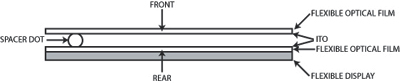
Fig. 1: A typical flexible resistive touch-screen construction shows the spacing between the layers.
Typical transparent conductive films include transparent conductive oxides (TCOs), such as indium-doped tin oxide (ITO), aluminum-doped zinc oxides (AZO), and metal-alloyed films (e.g., alternating layers consisting of Ag alloys and ITO) for EMI/RFI shielding purposes. Increasing the conductivity of the coating will increase the average attenuation level over the frequency range of 100 kHz through 20 GHz. Typical conductivities for transparent thin-film conductive coatings for this purpose range from 1 to 100 Ω/sq. Unfortunately, there is an inverse relationship between light transmittance and conductivity. At very high conductivities, metal-alloyed films offer better cost/ performance options over TCOs when applied to plastics. They can be cost effectively deposited in resistances down to 2 Ω/sq. while maintaining moderate total luminous light transmittance performance (typically >68%TL). The photopic transmission of metallic coatings quickly decreases as the conductivity increases. Additionally, metal alloys have an inferior mechanical and galvanic durability.
By contrast, TCOs become costly to apply to plastics for resistances below 30 Ω/sq., but can be applied to glass to values below 1 Ω/sq. A low-resistance coating on glass will offer high performance but cost more because it is deposited in a batch vacuum process rather than a web or continuous process. Additionally, most TCOs can be fully integrated into a multi-layered dielectric stack as part of a broadband anti-reflection (AR) coating. An AR coating reduces surface reflection losses and increases transmitted light. A fully enhanced TCO can have a total luminous reflection of a broadband white light source (e.g., illuminant D65) of less than 0.5%. Furthermore, the photopic absorption of TCOs tends to be very low, often less than a few percent at fairly high conductivities (i.e., <10 Ω/sq.). High transmissivity and low reflection of the materials used to construct the display/touch screen generally equate to higher display system luminance and efficiency.
ITO Replacement Coatings
ITO is the current leading transparent conductor used in displays and touch screens due to its high-performance optical, electrical, and durability properties. However, in order to reduce cost and improve performance, there are significant efforts being made in the marketplace to find a suitable replacement for ITO. Indium, the dominant component of an ITO coating, has a potentially limited availability and, as such, is subject to high costs and price volatility. ITO is also a brittle ceramic material and not ideal for highly flexible electronics. Materials such as silver conductive inks (for grid and irregular patterns), graphene, PEDOT-PSS, and other CNT-based conductive coatings are being developed and commercialized by a variety of organizations and companies.
For flexible electronics, these alternate materials offer the potential of greater durability when subjected to repeated bending. In order to offer a viable ITO replacement material, CNTs or silver conductive inks (or silver nanowires) must provide optical transparency in the range of 85–90% and sheet resistance in the 10–400-Ω/sq. range. The conductive layers of most resistive touch screens are in the ranges of 200–500 Ω/sq. For most flexible displays, the transparent conductive layers need to be approximately 1–50 Ω/sq. in order to create 100–300 x 10-6 Ω-cm pixel electrodes.3 In addition, the CNTs and silver nanowires must provide a material or processing cost advantage. ITO-coated films, with a cost range of $10–40 per square meter, are currently less expensive than most carbon- or silver-based nano-coatings. This may be partially due to the scale or production volume of ITO coatings compared to the alternative materials. This scenario is expected to change over the next few years with the advent of more efficient and larger-format R2R processing in the production of nano-materials. Current CNT-coated films offer a coating resistance in the range of 300–450 Ω/sq. with a transparency of 82%, which makes them viable candidates for ITO replacement materials used in touch screens. Silver nano-conductive coatings and grids can produce a sheet resistance of < 20 Ω/sq., allowing them to be used as flexible-display conductors. Table 4 shows the nominal transmission and reflection of transparent conductive coatings and grids used to construct resistive and capacitive touch screens and flexible displays.
Table 4: Typical transmission and reflection values are shown for various types of conductive meshes, grids, and films. [Openings per inch (OPI).]
| Conductive Ground Plane Mesh Composition |
Open Area % |
Photopic Transmittance Value |
Photopic Reflection |
| 50 OPI SS mesh Ag pl. & blk; 0.0012-in. wire diameter |
88.4 |
80–85 |
0.15–0.35 |
| 80 OPI SS mesh Ag pl. & blk; 0.0011-in. wire diameter |
83.2 |
77–83 |
0.15–0.35 |
| MEM100-80, etched Cu transparent conductive grid; 0.0005-in. grid width |
88–90 |
85 |
0.8–1.2 |
| CNT transparent conductive film |
100 |
82 |
<10 |
| Silver printed transparent conductive grid 100 OPI, 0.0008-in. grid width |
84.6 |
80 |
<8 |
| 10-ohms/sq ITO coating with no index matching |
100 |
85-88 |
7.0–10 |
| Index matched 10-ohms/sq. ITO coating |
100 |
>93 |
<0.5 |
Fine Conductive Grids (FCGs)
FCGs that offer low sheet resistance and good optical properties can provide X and Y coordinate locations for touch screens and flexible circuits or offer EMI/RFI shielding. A fine conductive grid pattern is typically made of conductively plated woven stainless steel or copper mesh, or with a printed/patterned metal coating on a surface of the substrate (e.g., PET). Both technologies have high open areas (e.g. > 85%) and excellent conductivities (e.g., from 100 to < 3 m Ω/sq.). For more details, please refer to our article, "Optical Enhancement and EMI Shielding for Touch Screens," in the May/June issue of Information Display or online atwww.information display.org.
Printed or selectively metalized conductive grids are typically produced via the deposition of silver nano-particles or conductive inks. Alternatively, metalized films can be patterned using photolithography, etching, or a similar technique. The process is amenable to R2R coating and results in flexible, highly conductive, transparent substrates. It should be noted that other touch-screen technologies, such as emerging optical touch-screen technologies based on sensors, eliminate the need for transparent conductive materials. As such, optical touch screens could be good candidates for the emerging flexible-display/touch-screen market. Currently, projected capacitive is the leading candidate.
Growth in Flexible Technology Means Growth in Related Materials
The growth in applications for flexible displays with touch screens is being driven by the market demand for lighter, less costly, and more functional user-interface devices. In addition to the material and process technologies used in the fabrication, flexible electronics can be applied to other emerging markets such as photovoltaics, smart cards, and solid-state lighting. Consequently, rapid market growth is forecasted for transparent conductive materials such as ITO, CNTs, and silver nano-coatings and conductive grids used in the production of flexible displays and touch screens.
References
1Display Bank Report (June, 2010). "Flexible Display Technology Trend Forecast (2008–2020).
2Ekkaia d., "Rise of the Flexible Touch Screen? Think Again," Multitouch Insider (2010).
3K. R. Sarma. Liquid Crystal Displays (CRC Press LLC, 2000). W. den Boer, Active Matrix Liquid Crystal Displays – Fundamentals and Applications (2005); http://www.engnetbase.com. •
Jeff Blake is Vice-President, Business Development and Richard Paynton is President of Dontech, Inc., Doylestown, PA. They can be reached at jblake@dontech.com and rpaynton@dontech.com, respectively, or at 215/348-5010.