Clearing the Road to Mass Production of OLED Television
Advanced material and process developments should help make printed OLED TVs commercially feasible.
by David K. Flattery, Curtis R. Fincher, Daniel L. LeCloux, Marie B. O'Regan, and John S. Richard
THE PROMISE of organic light-emitting-diode (OLED) technology has been to deliver displays that are more visually compelling and power efficient than liquid-crystal displays (LCDs) at a lower manufacturing cost. Today, most of this promise has been realized in small-format displays, but manufacturing cost and product price premiums persist. Furthermore, the feasibility of production on glass size comparable to that used for large-format LCDs has yet to be demonstrated.
Three key roadblocks must be removed for the successful mass production of OLED TVs. First, device performance in an actual display produced using manufacturing processes and architectures must achieve competitive thresholds for lifetime, efficiency, and color. Second, the processes and equipment required to accomplish this must be compatible with OLED production on Gen 8 (2.5 x 2.8 m) glass in order to enable competitive capital and fixed-cost productivity. Third, thin-film organic deposition and patterning techniques must significantly reduce the waste of expensive OLED materials. In this article, significant progress toward the removal of these roadblocks through the use of solution processing and particularly nozzle printing of large-format OLED displays will be reviewed.
Material performance in actual devices continues to rapidly improve through both process improvements and new material developments. The latest suite of solution materials achieves performance that now meets the minimum threshold required for commercial OLED television.
Over the last 15 years, dramatic increases in the scale of manufacturing have allowed LCDs to enjoy significant decreases in fixed and capital cost per square meter. Evaporative deposition of OLED material through a fine stencil mask is the generally established process. Unlike fine-metal-mask evaporation techniques, which have fundamental challenges to overcome for achieving production scale, the bulk of the equipment and tooling required for solution-processed OLED devices is commonly available at all scales. The critical exception is the nozzle printer, for which commercial systems have been produced up to full-size Gen 4 (0.7 x 0.9 m). The basic technology is fundamentally scalable, however, with engineering under way to deliver a full-size Gen 8 system.
Historically, 5–10 grams of OLED material are consumed for each gram of material evaporated onto the area of the substrate. Solution processing of coated and printed layers reduces consumption of materials to a fraction of this value. Through material and process developments that enable the solution processing of small-molecule OLED materials, the per-gram cost structure of most of the material layers has been made competitive with materials used for evaporation, which lowers the overall material cost when applied with higher efficiency.
When combined, the production of OLED TVs on full-scale equipment using solution processing and nozzle printing will deliver display performance equivalent to evaporation at an overall panel cost (without TFTs) that is reduced by 40–60%, depending on the scale achievable by evaporation techniques.
The Promise of OLED for Television
OLED displays have carried the potential of being an ideal technology for viewing large-format video from their inception. The basic structure of a stack of organic layers on the order of 200 nm thick that is directly emissive immediately invites the concept of an ultra-thin, high-contrast, fast-responding display. Combined with the laboratory demonstration of highly saturated colors and excellent power efficiency, these attributes implied that the development of large-format displays with cathode-ray-tube (CRT) quality and thinner-than-LCD format was simply an engineering challenge.
Additionally, the inherently simpler structure of OLED displays was expected to reduce manufacturing costs for OLED panels as compared to other technologies. Elimination of the light generation, distribution, polarization, and filtration elements of LCD panels was expected to far outweigh the cost of deposition of the organic layers and modification of the thin-film-transistor (TFT) array to support current-driven subpixels.
Commercialization of OLED technology has resulted in the achievement of some but not all of the potential of these displays. Cost and price have remained significantly above the LCD analogs; recent industry reports1 indicate that the average selling price for OLED modules runs ~3x that of the LCD equivalents.
OLED Material: From Test Coupons to Printed-Display Performance
The authors' company has been working for over 10 years in materials development for use in the solution processing of OLED devices. Core competencies in solid-state materials science, functional polymers, organic and organometallic materials synthesis, film coating, and formulations are all critical in tackling the inherently difficult task of printing organic electronic devices. One of the greatest challenges in manufacturing functional OLED displays is building a deep understanding of the strong interaction between OLED materials and the deposition process. Advances in both materials and process optimization have helped reduce the development cycle time. This cross-functional effort has resulted in small-molecule solution-based materials tailored to the nozzle-printing process that deliver OLED performance acceptable for commercial display applications.
An example of a typical development cycle, from conception of new compositions to integration in active-matrix OLED (AMOLED) displays, is outlined in Fig. 1. Transport, host, and emitter compositions are first tested in single, large-pixel, spin-coated test coupon devices. This platform is used because the devices are relatively simple and fast to prepare for the purpose of rapidly screening new materials. Through a series of experiments, the device architecture and layer-processing conditions of these test devices are adjusted to optimize color saturation, current efficiency, voltage, and lifetime. Color targets correspond to NTSC or sRGB standards so as to maximize the display color gamut. Power consumption is minimized to conserve power and slow the heat- and current-driven degradation of both the OLED and driving transistors. Loss of lifetime of the OLED device, which corresponds to dimming of emission over time arising from chemical degradation of one or more material components, is minimized.
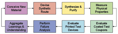
Fig. 1: The integrated material development process contains eight steps.
The spin-coated test coupon performance detailed in Table 1 is representative of a current typical material set. A common architecture was employed with identical layer thicknesses for indium tin oxide, hole/electron injection and transport, and cathode layers. Selectively optimizing individual layer thicknesses for each color can improve performance and is possible in the laboratory, but practical manufacture of an AMOLED display requires common layers. Consequently, all testing is performed using a common architecture to better predict real-world display performance. In order to achieve appropriate white balance, the common architecture selected is designed primarily to maximize blue color saturation, efficiency, and lifetime with concomitant reduction in red and green performance.
Table 1: Typical RGB performance using spin-coated test coupon devices is shown. T97 refers to the operating time that has transpired when the luminance output falls to 97% of its initial value when operated at constant current. Similarly, T50, mentioned further on in this article, means the time until a 50% drop. They are measured to assess both the potential for image burn-in (T97) as well as the time until full end-of-life (T50).
|
Color
|
|
Efficiency (cd/A)
|
Voltage (V)
|
CIE (x,y)
|
T97 (hours)
|
Lifetest Temperature(°C)
|
| Red |
900
|
21
|
5.8
|
(0.65,0.35)
|
800
|
24
|
| Green |
1850
|
89
|
3.9
|
(0.34,0.63)
|
900
|
24
|
| Blue |
900
|
6
|
4.8
|
(0.14,0.14)
|
500
|
32
|
aSimulates 200-nit FOS white with CIE = (0.28, 0.29), 40% AR, and 45% polarizer transmittance.
Each color was run at the luminance and color listed in Table 1, where the luminance values were selected. The data are not projected from accelerated testing. The luminance values were selected to simulate a bottom-emitting display running with a 200-nit white front-of-screen (FOS) brightness with 40% aperture ratio (AR) and 45% transmittance through a circular polarizer used for contrast enhancement. It should be noted that the subpixel luminance needs to be bright enough to compensate for these area and transmission losses. An elevated temperature was used to test the blue in this example because larger AMOLED displays will likely operate above ambient temperature.
New compositions that exhibit improved performance vs. incumbent "champion" materials are next tested in printed test devices. Transitioning candidate materials from spin coating to nozzle printing frequently requires substantial adjustments to formulations, architectures, and processing conditions. Materials that also show improved performance in printed devices are then fabricated into AMOLED displays. Extensive failure-analysis studies are conducted on both spin-coated and printed devices to pinpoint the material(s) in the device stack most responsible for any ensuing performance limitations. The data and understanding are used to conceive new material candidates, which begins the development cycle anew.
Typical nozzle-printed device performance results are shown in Fig. 2. Printed lifetimes are quoted at subpixel luminances that simulate 200-nit FOS white brightness. Even for blue, the most challenging color, lifetime exceeds 30,000 hours and should be sufficient for many display applications, including OLED TV. While, in general, the spin-coated results are indicative of final printed performance, the green material of Table 1 has not of yet been transitioned to a printable formulation. Hence, the green efficiency reported in Fig. 2 is significantly different from that shown in Table 1, as expected for two different materials.
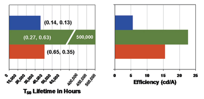
Fig. 2: Shown are printed bottom-emission test devices with no outcoupling enhancement, 200-nit FOS (white-point CIE 0.31, 0.32) with 40% AR, 45% transmission circular polarizer at 100% duty cycle. Lifetime data reported at 20°C.
Cost and Scale
LCDs have driven down cost per square-meter, in part through aggressive increases in the scale of manufacture. Figure 3 shows the relative capital productivity of the typical range of equipment used in the manufacture of TFT-LCDs. In general, equipment cost increases by about 30% for an increase in generation, while glass output increases 50–100%. Fixed cost, maintenance, and facilities costs follow similar trends. OLED manufacturing has had difficulty in following a similar strategy due to technical barriers encountered when scaling up the organic deposition process.
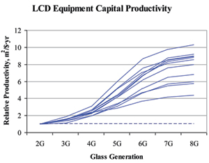
Fig. 3: TFT-LCD equipment capital productivity is compared to glass generation. Glass-area throughput for various types of equipment increases much faster than capital cost, resulting in a 4–10x improvement in capital productivity over the range of Gen 2 – Gen 8.3
AMOLED displays are almost exclusively manufactured on a smaller glass size than their LCD counterparts. OLED deposition is typically performed on glass sheets cut down after TFT manufacture. This is due primarily to the limitations of the fine-metal-mask evaporation process required to pattern the subpixel structure of the OLED. As mentioned above, an alternative to this deposition and patterning process, nozzle printing,2 has been developed in order to provide a readily-scalable technique for OLED manufacture.
Nozzle printing provides multiple continuous streams of OLED solutions that are drawn across the substrate at high speed using production equipment that Dai Nippon Screen Co. (DNS) developed in partnership with DuPont. The simple control requirements allow excellent uniformity to be achieved. Deposited volume is dependent only on flow rate (which is held constant) and speed, which are both readily controllable by developed technologies. Increasing the scale of the printing equipment is a relatively straightforward engineering task involving the optimization of the number of nozzles, speed, and acceleration of the printing head.
Because printing is a serial operation, the Total Average Cycle Time (TACT) of the equipment is a function of the display resolution and substrate layout as well as the substrate size. Since larger substrates are used to produce larger displays at lower resolution, the number of passes required by the printer does not increase as fast as generation size. Nevertheless, longer scan lengths and increasing scan counts will result in productivity decreases with increasing substrate size if all other parameters are held constant. Consequently, moderate nozzle count increases are planned for larger scale printers as illustrated in Fig. 4. Nozzle printers have been produced in full Gen 4 size with 15 nozzles. A single printer is capable of producing 10,000 sheets per month (benchmark 3.5-in. display) while depositing all three colors simultaneously. Similar printers with 30, 45, or 60 nozzles can maintain a 7,500–10,000 sheet output, as glass size is scaled up through Gen 5, 6, and 8.
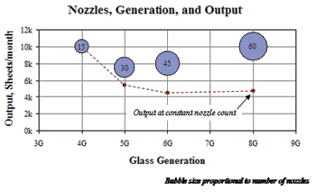
Fig. 4: Nozzle-printer output is shown for multiple generations of glass. Modest increases in nozzle count can maintain printer output in the target range of 7.5–10k sheets/month per printer. Estimates are based on benchmark display sizes of Gen 4 (3.5 in.), Gen 5 (12.1 in.), Gen 6 (17 in.), and Gen 8 (55 in.).
An additional consequence of the fundamentally serial nature of the printing process is the potential for non-uniformity of luminance across a display or substrate. The demonstration of the printing-process capability to meet these requirements has been the most significant milestone following the production of the Gen 4 multi-nozzle printer. As previously reported2 and illustrated in Fig. 5, the short-range uniformity of printed displays produced on this manufacturing equipment has exceeded the performance of commercial LCDs. All other steps required in the process developed by DuPont can be accomplished onstandard or modified LCD equipment where the economics of large glass sizes can be applied.
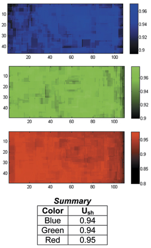
Fig. 5: Uniformity map data from multi-nozzle-printed AMOLED displays demonstrate superior short-range uniformity over production LCD benchmarks (SRU = 0.93).
Material Consumption and TACT
The consumption of OLED materials in the panel-manufacturing process plays a significant role in the economics of panel production. Thermal evaporation remains a relatively inefficient deposition technique where the vast majority of the material evaporated is not deposited over the substrate area. Metrics for defining deposition efficiency vary and can lead to confusion regarding actual material cost for panel manufacture. For this discussion, a material efficiency of 100% will be defined as using exactly the amount of material required to cover the substrate area with a layer of the target thickness. For example, if a transport layer with a density of 1.2 g/cm3is intended to be coated over the entire active area at a 15-nm thickness and the substrate area is 55,000 cm2 (Gen 8), the consumed mass of material is compared to (t x A x ρ) or (1.5 x 10-6 cm x 55,000 cm2/sheet x 1.2 g/cm3 = 0.1 g/sheet). If more than 0.1 g of material is consumed per sheet processed, the efficiency is less than 100%. It is a useful simplification to maintain this reference for more complex patterning of layers. If an emissive layer is patterned through a fine mask with a target thickness of 30 nm, the same basis can be used to calculate the material consumption; even though the material is required on less than 30% of the substrate area, consumption for that layer will be similar.
Using this reference, the amount of material consumed per layer can be described as the multiple of that which would be required if the theoretical 100% efficiency is achieved. This parameter has the dimensionless units of g/g or the number of grams consumed to deposit a layer over the grams required to coat the entire substrate with a layer of the same thickness. Typical evaporative processes require 5–10 grams of material per gram deposited on the area of the substrate. This parameter is significantly impacted by the evaporator design with classic long-throw, point-source evaporators requiring the highest material waste. Shorter-throw evaporators with linear sources have been demonstrated to reach the 5 g/g metric. Some new evaporator sources claim efficiencies in the 2–3 g/g range, although these efficiencies have not been attempted in production.
Solution-processed material efficiencies vary depending on the deposition technique employed. For unpatterned coatings, such as hole-injection layers, efficiency is largely determined by the ratio of slot coater priming to coating time. Priming of the coating head is accomplished by depositing material on a priming roll in order to wet the die lips and prepare the die to deposit a defect-free film. Typically, the priming of the coating head is accomplished for a fraction of the time required for coating the substrate, so efficiencies in the range of 1.1–1.3 g/g are readily achieved.
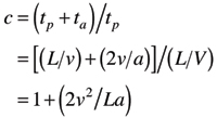
Printing efficiency is more complex and interacts with other printing parameters. Nozzle printing employs a continuous flow of ink through the printing orifice and results in material waste when the printing head is accelerating or decelerating off of the substrate. The optimization of scan time and material efficiency is a key part of nozzle-printing-equipment engineering.
Acceleration of the nozzle print head is typically constrained by the mechanical system employed to drive the head traverse. For a given acceleration, an optimum speed can be established for any given scan length that will provide the shortest scan time:
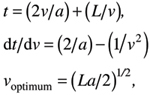
where t is the scan time, v is the head velocity, a is the head acceleration, and L is the scan length. Similarly, the material consumedvs. printed (g/g metric) can be estimated based on the total scan time over the time spent printing. This is simply expressed as
where c is the material consumed vs. theoretical, tp is the printing time, and ta is the acceleration time.
From the above equation, it is clear that an increase in acceleration and/or scan length will improve efficiency and a decrease in scan velocity will improve efficiency. Any printer optimized for TACT alone will give a consumption of 2 g/g since cycle time is optimized when tp = ta. This leads to a fundamental trade-off in printer design to find a working value of scan velocity that will deliver acceptable TACT at good efficiency. For the Gen 4 printer configuration, the operating point has been selected at 10 g acceleration and 5-m/sec velocity, giving 1.6 g/g scan consumption (for full-sheet coverage) with a scan time of about 300 msec.
The summary of these material-consumption comparisons is that while evaporated layers typically consume 5–10 g of material per gram of material needed to coat the substrate, solution-processed layers consume 1–1.3 g for coated layers and 0.6–2.0 g for printed layers, depending on the selected architecture. For typical RGB printed layers, consumption of the emissive material is less than 1 g/g since the printed area is significantly less than the substrate area (Fig. 6).
Fig. 6: Design parameters for nozzle printing require balancing optimum TACT with material efficiency to deliver the lowest total cost.
Cost of Manufacture
By combining the material, capital, and fixed-cost assumptions outlined above, projections of manufactured cost for the OLED panel can be generated. The following charts compare projections for evaporation on cut-down substrates as well as projections that assume evaporation can scale to the full-sheet processing. Costs are for OLED fabrication only and exclude TFT and module components.
Cost of manufacture for nozzle-printed OLEDs is projected to be about 30% below the incumbent LCD cost and almost 50% below equivalent evaporated panels, as shown in Fig. 7. The cost savings are a result of lower material consumption, lower capital cost, and lower fixed cost due to reduced maintenance and tooling required for printing equipment. When costs of full Gen 8 solution processing are compared to cut-down processing for evaporation, the differential increases to almost 60%.
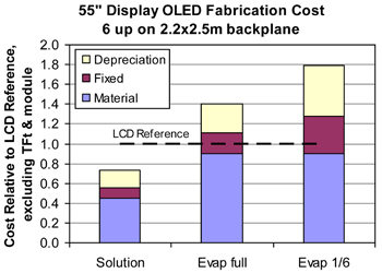
Fig. 7: A cost comparison for evaporation shows full and cut-down substrates. Reference LCD comes from third-party industry cost models provided by iSuppli and DisplaySearch.
"Solutions" for OLED Manufacturing Costs
OLED-TV manufacture can be practically accomplished through solution processing. Material developments have delivered performance that meets the threshold for television requirements and process developments can meet manufacturing cost targets. Nozzle printing is a flexible technology that uses materials efficiently and can be scaled to Gen 8 glass size to enable OLEDs to enjoy the same economies of scale that have enabled LCDs to become the dominant display technology. These advancements will allow the myriad benefits of OLEDs to be delivered while significantly reducing manufacturing costs compared to LCD incumbents.
References
1"Q2 '11 Flextech Alliance Business Conditions Report," DisplaySearch, p.18 (July 2011).
2R. Chesterfield et al., "Solution-Coating Technology for AMOLED Displays," Information Display 27/1, 24-30 (2011).
3Data aggregated from industry LCD cost models and vendor quotations. •