A Flexible Universal Plane for Displays
FlexUPD is the Industrial Technology Research Institute's flexible-universal-plane solution for quality flexible displays and other non-display applications. Using FlexUPD technology, ITRI successfully integrated a flexible TFT backplane with AMOLEDs and received The Wall Street Journal's 2010 Technology Innovation Gold Award.
by Janglin Chen and Jia-Chong Ho
FLEXIBLE DISPLAYS represent a megatrend within the next-generation display market because of their light weight, sturdiness, and shape-forming capabilities. In order to create flexible displays, however, it is necessary to develop a corresponding flexible substrate material, along with a process that includes chemical resistance, thermal stability, endurance in high temperatures and pressures during the TFT process, and moisture-barrier properties. Active-matrix organic light-emitting-diode (AMOLED) technology is among the most attractive display technologies for building on a flexible substrate because it is self-emissive and has attributes such as high video rate, wide color gamut, low power consumption, and, most importantly, simplicity in structure.1
However, although the idea of flexible AMOLED displays is intriguing, the development of the necessary flexible substrate remains a challenge. Many substrates, such as ultra-thin glass, plastic, and stainless steel, have been tried but without commercial success because they lack the proper surface properties, thermal stability, or mechanical properties, or because they cannot sustain the stringent TFT processing conditions.2-4 LG has focused on the development of metal-foil substrate for flexible displays because of its high thermal stability, low cost, and low coefficient of thermal expansion (CTE).5 However, the surface of the foil is too rough to be used directly as a flexible substrate and additional polymer coating for surface smoothing is needed, which makes the technology less attractive. Thin glass as a flexible substrate has also been tried, but has not met with commercial success due to its brittleness. Plastic films on glass, which are being developed by many companies and research groups, are now considered as one of the most promising substrates for flexible displays.
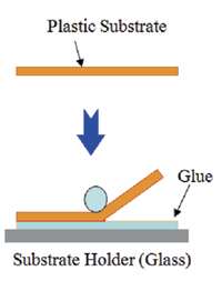
Currently, plastic substrates are prepared by laminating or coating a plastic layer on glass carriers, followed by fabricating TFT devices on the substrates, then releasing the substrate with a TFT backplane from the glass. The most daunting challenges of these approaches are finding the right substrate material and also developing the de-bonding technology to remove the plastic film from the glass. As shown in Fig. 1(a), a representative structure for a laminating approach consists of a plastic layer such as PC, PET, PEN, PES, PI, etc., adhesive glue, and glass. This approach, in general, has issues of poor alignment, residual glue, and process temperature limitation, which have rendered the plastic film lamination approach less feasible.
With the approach of coating a plastic layer onto the glass substrate, as shown in
Fig. 1(b), those issues have been eliminated or made less severe. However, the de-bonding of the flexible TFT backplane is still a challenge. Recently, two de-bonding methods for the coating-type substrate technology have been developed; namely, the Electronics-on-Plastic by Laser Release (EPLaR) process developed by Philips
6,7 and the FlexUPD Flexible Universal Plane for Display (FlexUPD) by ITRI.
8 The EPLaR technique uses a laser to remove the substrates from the glass carrier. The equipment cost of the laser is high and the throughput is slow. ITRI's FlexUPD approach uses a de-bonding layer for release of the substrate and should be the more viable approach to enabling the mass production of thin, low-cost flexible displays. The possible value of the process was recognized just recently, when ITRI's FlexUPD was presented with a Gold
Wall Street Journal 2010 Technology Innovation Award (the top prize) for innovation, potential impact, and promise for commercialization.
 (a)
(a) 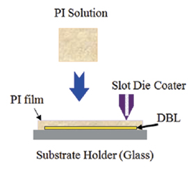 (b)
(b)
Fig. 1: Flexible Universal Plane Technology relies on two key innovations: (a) the substrate and (b) a de-bonding layer (DBL).
By using FlexUPD technology, flexible displays can be processed in current TFT manufacturing facilities, many of which have been fully depreciated. Consequently, the capital investment in order for the industry to quickly adopt this technology is low. The developed FlexUPD flexible substrate technology is a platform technology, which allows it not only to be applied for displays, but also for non-display applications. In principle, the FlexUPD technology can be used for OLEDs, LCDs, EPDs, and other display types. And it can be applied to applications such as flexible OLED lighting, flexible photovoltaics, flexible sensor arrays, flexible x-ray sensor arrays, and more.
Flexible Universal Plane for Display Technology
ITRI developed the FlexUPD plastic substrate technology by coating a polyimide solution directly onto the glass substrate with a de-bonding layer (DBL) as shown in Fig. 1(b), followed by fabricating TFT devices on the said substrate. Then the substrate was released from the glass. The DBL provides a weak interface between it and the plastic film, which allows the film to be easily released after the TFT process. Two key innovations make the FlexUPD a success: the flexible substrate material and the de-bonding technology.
Flexible Substrate Material
Polyimide (PI) is an excellent choice for a coating-type substrate material due to its good thermal and chemical resistance. In general, PI is prepared by first reacting a diamine monomer with a dianhydride monomer in a polar solvent to prepare a precursor poly(amic acid) (PAA). Then the PAA is coated on glass and subjected to thermal treatment for imidization. Typically, the thermal imidization is run at high temperature (>300oC) and the total processing time is longer than 3 hours, which are rather stringent processing conditions. At ITRI, a colorless polyimide is synthesized with non-fluoro monomer, which can be processed at <250oC in less than 1.5 hours. Moreover, it exhibits good light transmittance (90%), high glass-transition temperature (Tg>300oC), and good chemical resistance. The material characteristics of PAA-type PI and ITRI's PI are compared in Table 1.
Table 1: PAA-type PI and ITRI's PI are compared in terms of chemical resistance, transparency, and other attributes.
| |
PI (PAA type) |
ITRI's PI |
| Tg (°C) |
>300°C |
>300°C |
| CTE (ppm/°C) |
30–40 |
50–60 |
| Chemical resistant |
Excellent |
Good |
| Transparency (%) |
<30 |
>90 |
| Surface visibility |
Both sides visible |
Top side visible |
| Maximum drying temperature |
>300°C |
<250°C |
| Time of process |
>3 hours |
<1.5 hour |
A new inorganic-dominated silica/polyimide (PI) hybrid film has also been successfully developed for the high-performance substrate.9 The high inorganic content (>60 wt.%) brings high modulus, thermal resistance, and low coefficient of thermal expansion (CTE) to the film. Table 2 summarizes the properties of the silica/PI hybrid film.
Table 2: Properties of the silica/PI hybrid film include a 90% light transmittance at 550 nm.
| Sample name |
SiO2/PI hybrid film |
| Tg (°C) |
>400
|
| CTE (ppm/°C) |
28
|
| Young's Modulus (GPa) |
4.3
|
| Light transmittance (% at 550 nm) |
90
|
| Haze |
0.01
|
Flexible Substrate De-Bonding Technology
This novel flexible-substrate technology is compatible with existing TFT infrastructures and processes. Figure 2 is a schematic illustration of the de-bonding technology, which differs from conventional laminating technology in two aspects. First, the solution-type PI is coated directly onto the glass carrier with a de-bonding layer (DBL). The distortion of the PI substrate due to thermal expansion can be kept to a minimum throughout the TFT process and the PI film can be released from the glass after the TFT process. Secondly, unlike the pre-formed foil substrates, the thickness of the coated PI film can be easily controlled by metering the solution lay-down.
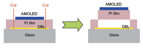
Fig. 2: In this flexible-substrate schematic, at left, the edges of the PI film are in direct contact with the glass during processing, which reduces the possibility of thermally induced misalignment. Cutting is done along the circumferences of the PI layer inside the edge of the DBL. Then, due to the weak adhesion of DBL with PI film, the PI layer can be easily separated, as shown at right.
As shown in Fig. 2, the edges of the PI extend over the underlying DBL and are in direct contact with the glass, which allows the PI layer to be securely adhered to the glass carrier throughout TFT processing, where thermally induced misalignment might otherwise occur.
With the developed PI and DBL, the PI substrate can be securely adhered to the glass carrier during the entire TFT process so that there is no misalignment problem. Besides, after the designed TFT processes are completed, the PI substrate with a TFT backplane can be easily separated from the glass. For this de-bonding method to be applied in mass production, an automatic flexible-substrate de-bonding procedure is needed. Consequently, a custom-designed flexible-substrate de-bonding apparatus facilitated with a vacuum system was developed for releasing the flexible display. The prototype of the apparatus is shown in Fig. 3.
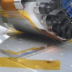
Fig. 3: This flexible display de-bonding apparatus is a prototype.
Based on this novel flexible-substrate technology, we were able to develop flexible TFT backplane technology, flexible OLED technology, and flexible touch technology.
Flexible Substrate for AMOLED Displays
When a plastic substrate is used for the flexible OLED application, the water-vapor transmission rate (WVTR) of plastic substrate becomes critical. A general PI film has a WVTR of 5 g/m2/day and higher, whereas for OLED applications, the WVTR of the substrate has to be lower than 4 x 10⁻⁵ g/m2/day. In order to overcome such a deficiency, a barrier layer was introduced. With our barrier technology, the WVTR of PI can be improved to less than 4 x 10⁻⁵ g/m2/day. Moreover, this barrier property suffered only a minor drop, to 8 x 10⁻⁵ g/m2/day, after the flexible panel had been bent 1000 times at a radius of 5 cm. The WVTR of intrinsic PI and PI with the barrier is compared in Table 3.
Table 3: The water-vapor transmission rates of intrinsic PI and PI with a gas barrier are compared.
| |
|
Testing Environment 60°C, 90%RH
|
| Sample |
Film thickness (μm) |
Before bending
WVTR (g/m2/day)
|
After bending
(@ R=5 cm, 1000 times)
WVTR (g/m2/day)
|
| Intrinsic PI |
15–30
|
> 5
|
>5 (measured using MOCON instrument10) |
| PI with gas barrier |
0.3–1.5
|
4 x 10⁻⁵
|
8 x 10⁻⁵ (measured using calcium test11) |
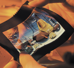
In our flexible-display construction, the top-gate TFT arrays were first integrated with a two-transistor, one-capacitor circuit in the backplane, and then the color OLED was deposited on the TFT backplane to form an AMOLED display. Photographs of a 4.1-in. (108 x RGB x 240) flexible color AMOLED display under bending (curvature radius ~ 5 cm) and a 6-in. (320 x RGB x 240) flexible color AMOLED display are shown in Figs. 4(a) and 4(b), respectively. The total thickness of the 6-in.flexible AMOLED display is about 65 μm, which can be bent at a curvature radius of 5 cm for 15,000 times without deterioration in performance.
 (a)
(a) 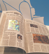 (b)
(b)
Fig. 4: (a) A flexible 4.1-in. (108 x RGB x 240) color AMOLED and (b) a 6-in. (320 x RGB x 240) flexible color AMOLED in a simulated newspaper demonstration.
Flexible Touch AMOLED Display
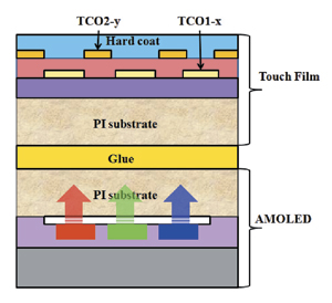
A flexible touch AMOLED display was also successfully developed by ITRI. With the approaches described above, the flexible TFT backplane, the flexible OLED, and the flexible touch film could be integrated on the transparent PI substrate using FlexUPD technology. Figure 5(a) shows schematically the structure of the flexible color AMOLED with ultra-thin touch-sensing film. Profiles of the signal intensities of the touch-sensing panel with and without finger touching were measured and plotted as shown in Fig. 5(b). With a high S/N ratio, the touch signal can be reliably distinguished from noise. We have successfully integrated and demonstrated the performance of an ultra-thin touch-sensing film with a flexible color AMOLED as shown in Fig. 5(c), which, to the best of our knowledge, is the first flexible touch AMOLED display demonstrated in the world.
 (a)
(a) 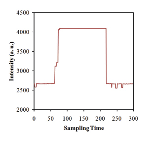 (b)
(b) 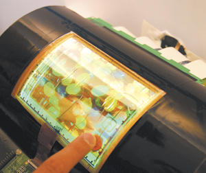 (c)
(c)
Fig. 5: (a) An integrated structure of a flexible AMOLED display and projective-capacitive touch-sensing film. (b) Signal intensities of the touch-sensing panel with and without finger touch. (c) A prototype of the flexible touch AMOLED display in a curved configuration.
A Technology with Scalability
Using the novel FlexUPD technology, ITRI was able to demonstrate a flexible AMOLED display. The technology used includes a flexible substrate material, a de-bonding layer material, de-bonding process, flexible TFT process, and flexible OLED process. With ITRI's approaches, the PI substrate can be used in high-temperature TFT processes, and the alignment shift can be controlled within 2 μm. In addition, the flexible display can be easily released from the glass carrier without any damage. We believe that the technology can be readily scaled up to produce larger-sized flexible substrates (larger than Gen 4) on current TFT display-manufacturing facilities.
Acknowledgments
The authors appreciate contributions from the members of both the Display Technology Center (DTC) and the Material and Chemical Research Laboratories (MCL) at the Industrial Technology Research Institute (ITRI).
References
1T. Serikawa and F. Omata, "High-Quality Polycrystalline Si TFTs Fabricated on Stainless-Steel Foils by Using Sputtered Si Films,"IEEE Trans. Electron Dev. 49, 820–825 (2002).
2D. U. Jin, J. K. Jeong, T. W. Kim, J. S. Lee, T. K. Ahn, Y. K. Mo, and H. K. Chung, "World's Largest (6.5 in.) Flexible Full-Color Top-Emission AMOLED Display on Plastic Film and Its Bending Properties," SID Symposium Digest 40, 1516-1519 (2009).
3S. D. Theiss and S. Wagner, "Amorphous Silicon Thin-Film Transistors on Steel Foil Substrates," IEEE Electron Device Lett. 17, 578–580 (1996).
4S. Y. Kim, K. Kim, K. Hong, K. S. Jun, and J-L. Lee, "Mechanism of Peel-Off of Metal Substrate for Flexible Devices," SID Symposium Digest 40, 1516-1519 (2009).
5S. H. Paek, Y. I. Park, C. H. Park, Y. S. Lim, S. l. Shin, C. D. Kim, and Y. K. Hwang, "Distinguished Paper: Flexible Display Technology for Mass Production Using Improved Etching Technology," SID Symposium Digest 41, 1047-1049 (2010).
6E. I. Haskal, I. D. French, H. Lifka, R. Sanders, P. T. Kretz, E. Chuiton, G. Gomez, F. Mazel, C. Prat, F. Templier, M.D. Campo, and F. Stahr, "Flexible OLED Displays Made with the EPLaR Process," Proc. Eurodisplay '07, 36-39 (2007).
7I. French, "Flexible e-Book," SID Symposium Digest 40,100-103 (2009).
8C. C. Lee, Y. Y. Chang, H. C. Cheng, J. C Ho, and J Chen, "A Novel Approach to Make Flexible Active Matrix Displays," SID Symposium Digest 41, 810-813 (2010).
9J. M. Liu, T. M. Lee, C. H. Wen, and C. M. Leu, "High Performance Organic-Inorganic Hybrid Plastic Substrate for Flexible Display and Electronics," SID Symposium Digest 61, 913-916 (2010).
10D. S. Wu, T. N. Chen, E. Lay, C. H. Liu, C. H. Chang, H. F. Wei, L. Y. Jiang, H. U. Lee, and Y. Y. Chang, "Transparent Barrier Coatings on High Temperature Resisting Polymer Substrates for Flexible Electronic Applications," J. Electrochem. Soc. 157 (2), C47-C51 (2010).
11P. F. Carcia, R. S. McLean, M. H. Reilly, M. D. Groner, and S. M. George, "Ca Test of Al2O3 Gas Diffusion Barriers Grown by Atomic Layer Deposition on Polymers," Appl. Phys. Lett. 89, 031915 (2006). •
Janglin Chen and Jia-Chong Ho are with the Display Technology Center (DTC), Industrial Technology Research Institute (ITRI), in Hsinchu, Taiwan. Janglin Chen, ITRI Vice-President and General Director of DTC, can be reached at janglinChen@itri.org.tw.