Optical Enhancement and EMI Shielding for Touch Screens
The demand for touch technology has infiltrated almost every device involving a display. As such, engineers are being asked to incorporate touch screens into designs for an everincreasing range of applications and environments. Successful projects will provide the optimum balance of readability and electromagnetic compatibility.
by Brian E. Herr, Jeff Blake, and Richard D. Paynton
ELECTRONIC DISPLAYS with touch-screen interfaces are now commonplace in marine, military, and mobile applications. In these demanding environments, the necessary high-ambient-light readability and electromagnetic compatibility (EMC) can be most efficiently achieved through enhancements to commercial-off-the-shelf (COTS) components. System designers must maintain EMC and enhance COTS touch screens that otherwise would degrade the high-ambient readability of the display to an unusable level. Electromagnetic radiation emitted by the device, or electromagnetic susceptibility to radiation somewhere in the environment, are also present significant challenges because the face of the display still needs to be transparent. The term EMC in general denotes the ability of an electronic system to function within its operational environment without emitting unacceptable levels of electromagnetic radiation or failing to perform due to the influence of an external electromagnetic field in its working environment.
The technology to modify display systems for both high-ambient-light readability and EMC compliance is readily available. Touch screens integrated into display assemblies can be configured to provide an electromagnetic interference (EMI) shielding conductive ground plane and contrast-enhancement features to address these issues. The enhancements described in this article focus on resistive touch-screen technology and its integration into high-ambient-light-readable liquid-crystal-display (LCD) assemblies, but are applicable to other touch-screen technologies as well.
High-Ambient-Light Readability
High-ambient-light readability is a performance characteristic of a display system that is directly dependent upon three factors: the available luminance of the display, the amount of ambient illuminance in the environment, and the amount of ambient light reflected by the display and front optical components, including the touch screen. To be truly labeled as "high ambient readable," the display system, when energized, must be readable in the worst-case conditions for the product's intended use (e.g., direct sunlight). Surface reflections, which occur at interfaces between mediums of differing refractive indices, degrade contrast by reflecting the incident light. For instance, plain, clear, uncoated glass in air has a photopic reflectance of 4.25% on each surface due to the difference in refractive index between the glass and air. The even higher-refractive-index conductive coatings used in constructing most resistive touch screens can reflect up to 8–10% per resistive layer due to the high refractive index of the conductive layer and the quarter-wave effect of the thin-film coating stack. Consequently, the performance loss of a resistive COTS touch-screen assembly can exceed 24% due to the reflection caused by index-mismatch issues and the optical stack configuration (Fig. 1).
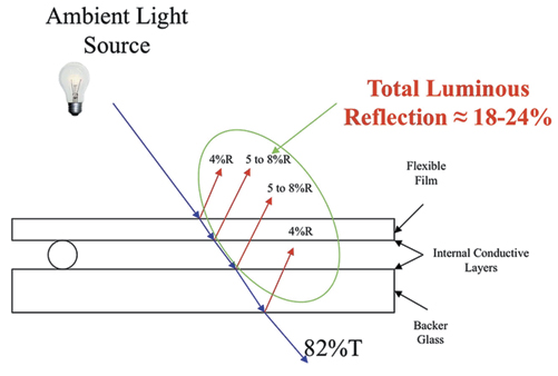
Fig. 1: Luminous reflection is shown in a standard resistive touch-screen construction.
Contrast Issues with COTS Displays and Touch Screens
Using the VESA (Video Electronic Standards Association) Flat Panel Display Measurement (FPDM 2.0) standard and military standard MIL-L-85762A as a basis for the test procedures, the optical performance profile of the display can be accurately quantified. (Many commercial procedures and practices do not allow for direct comparisons and correlations between products and companies.) A good contrast measurement will quantify the disparity between the activated or "on" areas of the display and the dark or "off" areas in a standardized high-ambient-light environment. Contrast will decrease significantly with increased reflections in the display system (e.g., the insertion of a highly reflective touch screen) [see Eq. (1)].
Contrast Ratio or Luminance Ratio =
Total luminance of the image, including any
background or reflected light, as measured
in the specified lighting conditions divided
by the luminance of the background, or
dimmer area, including any reflected light
and any stray display emissions, measured
in the specified lighting conditions. Eq. (1)
Dark Ambient:
Contrast Ratio = Light Area of Display /
Dark Area of Display = Light / Dark
High Ambient:
DL = Lambertian Component of the
Diffuse Reflection, S = Specular Reflection,
DH = Haze Component of the Diffuse Reflection.
Contrast Ratio = (Light + Reflections) /
(Dark + Reflections) = (Light + DL +
S + DH) / (Dark + DL + S + DH) =
(Light + D + S) / (Dark + D + S).
Resistive touch screens have four major interfaces, each of which either goes from air to an optical medium or, conversely, from an optical medium to air, all of which are sources of reflections. Reflection problems are further compounded because the resistive touch screen comprises plastic substrates with hard coatings and thin-film coatings on both rigid and flexible optical materials (either glass or plastic) that create additional material interfaces and sources of reflection. Hard coatings are thick-film coatings (typically > 0.012 mm in thickness) that improve the durability of polymer layers (e.g., abrasion-resistant coatings) and are typically applied as a wet chemistry. Thin-film coatings, used to convert reflected light to transmitted light and to create transparent conductive coatings, are typically 100–3000 Å in thickness and are either applied by sol-gel (chemical solution deposition) or high-vacuum-coating processes. A better understanding of the cumulative effects of the surface reflections for the bulk or thick-film materials can be attained using the Fresnel equation for normal reflections:
R = RS = RP = [(n1 – n2)/(n1 + n2)]2. Eq. (2)
RS = S polarization component
RP = P polarization component
n = index of refraction
When applied for normal incident light to the first surface interface where the initial medium is air (n1 = 1.0) and the exit medium is an acrylic hard coating (n2 = 1.5), the result is a value of 4% for the first surface reflection. The reflection increases due to refractive index differences between the conductive thin-film coating (i.e., the active conductive layer inside the touch screen), the substrate, and air. The reflection can be reduced by "index matching" of the conductive coatings (e.g., adding a dielectric layer to the conductive coating to lower its reflection components). For a resistive touch screen, the conductive layers can only be partially optimized or index-matched (see Fig. 2) because the surfaces of the active portion of the touch screen must remain conductive.
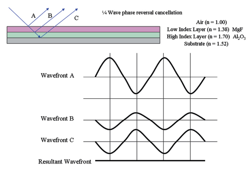
Fig. 2: Above is an example of a basic index-matching coating to air.
Design Considerations: Optical Enhancements to Touch Screens
Antireflective, antiglare coatings, polarizers, and optical bonding:
In order to reduce the surface reflections in a touch-screen display system, each interface must be considered. By lowering the refractive index of the touch-screen surfaces, an antireflective coating on both the front and rear surface can reduce surface reflections by approximately 7% by reducing the inherent 4.25% reflection per surface to less than 0.75%. The total reflections for the outer surfaces will be reduced from 8.5% to < 1.5%. However, there can be a wide range of internal reflections in a COTS touch screen (i.e., < 2% to > 8% per interface). A thin-film anti-reflective coating cannot be directly deposited in a vacuum to the completed COTS resistive touch screen. The deposition process would cause the air gap between the flexible membrane and the rigid support layer to collapse, which would result in varying degrees of plastic deformation around the spacers and the degradation of the touch screen's optical and electrical integrity. For this reason, it is common to apply a conductive coating to an optical substrate, then to laminate it onto the surface of the touch screen. The most cost-effective method is to apply a flexible-film lamination (0.003–0.009 in. in total thickness) to one or both surfaces of the touch screen. Common optical substrates include polyethylene terephthalate (PET), cellulose triacetate (TAC), and glass. The flexible substrates can be coated with acrylic or silane-based hard coatings to improve mechanical durability and antiglare coatings to scatter specularly reflected light. Considerations for carrier film selection are index of refraction, durability, cost, and birefringent properties.
Optically coupling the rear surface of the touch screen with the front surface of the display using an index-match bonding adhesive is becoming an increasingly popular method to improve high-ambient-light readability. By using optical bonding, two reflective surfaces are eliminated, thereby increasing contrast. Additional benefits include elimination of internal surfaces where condensation can occur as well as better shock and vibration performance.
As shown in Fig. 3, internal reflections, coupled with ambient light reflected from the front surface of the display or rear surface of the touch screen, will reduce contrast and viewability. To address this issue, a circular polarizer (CP) can be integrated into the front surface membrane of the resistive touch screen to suppress internal reflections. The CP is a linear polarizer combined with a quarter-wave retarder. Unpolarized ambient light entering the display from the outside first passes through a linear polarizer (the first layer of the circular polarizer). When the light, now linearly polarized, passes through the quarter-wave retarder, it is separated into two equal components that are one quarter wavelength out of phase with one another (i.e., the phase relationship is such that the leading component is one quarter wavelength ahead of the lagging component). When this light strikes a specularly reflecting surface (e.g., the conductively coated internal layer of a resistive touch panel) and is reflected, the phase relationship between the two wave components is reversed. Therefore, the previously lagging component is now one quarter- wavelength in front. It then re-enters the retarder. The retarder realigns the two components and the resultant light is oriented 90¼ from the original light. Thus, when it then passes through the linear polarizer again, it is blocked because it is 90¼ opposite to the linear polarizer. In this way, unwanted reflected ambient light originating outside the display is separated from the desired light emitted by the display. This methodology can eliminate almost all (99%) internal reflections by introducing a phase shift of the orthogonal components of the polarized light that is reflected off the internal layers of the touch screen.
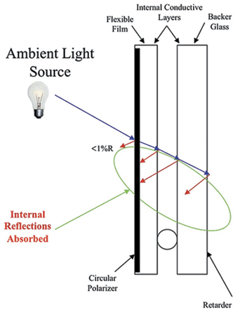
Fig. 3: Polarized construction details show where internal reflections are absorbed.
By minimizing reflection loss, contrast and therefore high ambient readability of the display is greatly increased. When integrating a CP into a touch screen, the polarization angle must be aligned with the polarization angle of the display. Unfortunately, birefringent materials used in touch-screen construction (i.e., PET) may interfere with the function of the CP and should be addressed earlier in the design.
Electromagnetic-Interference Shielding
For EMI shielding, a typical touch-screen-enabled display assembly is constructed with a Faraday cage – a continuous electrically conductive enclosure that surrounds the equipment and attenuates transmitting electric fields to a desired level. Metalized enclosures form most of the Faraday cage in typical display assemblies, but obviously must leave the display face open and viewable. Therefore, conductive ground planes (CGPs) with satisfactory transparent properties must be installed in the display's optical path to complete the Faraday cage and function as an EMI shield. If this element of the Faraday cage is not properly terminated (e.g., the shielded touch screen is only terminated on one or two corners) this portion of the shield could act as an antenna and re-radiate an undesired electrical field.
Common EMI shielding techniques for adding conductive properties to an optical substrate include integration of transparent conductive coatings or a fine conductive grid of wires. Electrically conductive, optically transparent ground planes pass the dominant portion of the visible spectrum (i.e., 380–780 nm). The properties of transmittance and conductance can be adjusted or tuned to fit a specific application. All transparent conductive materials require an optical substrate as a carrier. To avoid the potential for birefringence and moiré (see Fig. 6), it is important to review and understand the properties of the materials and components that compose a COTS touch-screen display assembly as well as the CGP, due to the interrelationships between the optical and shielding performance of the system. The EMI shields will attenuate the visual light transmittance from 3% to 55%, depending on the specific technology and configuration employed.
Transparent Thin-Film Conductive Coatings
Transparent thin-film conductive coatings offer excellent optical and moderate EMI shielding properties. Typical transparent conductive films include transparent conductive oxides (TCOs) such as indium tin oxide (ITO) and metal alloyed films (e.g., alternating layers consisting of Ag and ITO). Increasing the conductivity of the coating will increase the average EMI attenuation level over the frequency range of 100 kHz – 20 GHz. Typical conductivities for transparent thin-film conductive coatings for this purposed range from 1 to 100 Ω/sq. Unfortunately, there is an inverse relationship between light transmittance and conductivity. Metal alloyed films offer better cost/performance options over TCOs, especially when applied to plastics. They can be cost-effectively deposited on plastics in resistances down to <3 Ω/sq. while maintaining moderate total luminous light transmittance performance (i.e., >68%TL). However, the photopic transmission of metallic coatings quickly decreases as the conductivity increases due to the high absorption component and increased reflection as compared to TCOs. (100% = Absorption + Reflection + Transmission). For example, a 10-Ω/sq. dielectrically enhanced TCO (ITO) coating has <3% photopic absorption and <0.5% photopic reflection, providing a total luminous transmittance of >96%. The metallic coating equivalent transmittance is only nominally 83% due to the >3% reflection and approximate 13% absorption. Additionally, metal alloys have an inferior mechanical and galvanic durability.
By contrast, TCOs become costly to apply to plastics for resistances below 30 Ω/sq., but can be applied to glass to values below 1 Ω/sq. A low-resistance coating on glass will offer high performance but will cost more because it is deposited in a batch vacuum process rather than a web or continuous process. Additionally, most TCOs can be fully integrated into a multi-layer dielectric stack as part of a broadband antireflection (AR) coating. This is commonly referred to as "index matching." An AR coating reduces surface reflection losses and increases transmitted light. A fully enhanced TCO can have a total luminous reflection of a broadband white light source (e.g., illuminant D65) of less than 0.25%. Furthermore, the photopic absorption of TCOs tends to be very low, often less than a few percent at fairly high conductivities (i.e., <10 Ω/sq.), allowing a total luminous transmittance (TL) of > 95%.
Fine Conductive Grids (FCGs)
FCGs are CGPs that offer excellent EMI shielding and good optical properties (see Table 1 for relative shielding properties).
Table 1: The typical shielding effectiveness of two different technologies – indium tin oxide and plated wire mesh – is compared.
| Frequency |
10 Ω/sq.
ITO (db)
|
80 Mesh
Plated (db)
|
|
H Field
|
| 100 kHz |
0
|
15
|
| 1 MHz |
1
|
32
|
|
E Field
|
| 100 kHz |
72
|
86
|
| 10 MHz |
36
|
81
|
|
Plane Wave
|
| 100 MHz |
24
|
71
|
| 1 GHz |
25
|
58
|
| 10 GHz |
18
|
34
|
A typical fine-conductive grid pattern is made of plated woven stainless-steel or copper mesh, or with a patterned metal coating on the surface of a substrate. Both technologies have high open areas and excellent conductivities (e.g., 100 to < 3 mΩ/sq.). Plain-weave mesh is constructed with fine wires (e.g., 0.0005–0.002 in.) crossing alternately over and then under one another with adjacent wires 180° out of phase (similar in construction to a window screen but significantly finer), as shown in Fig. 4.
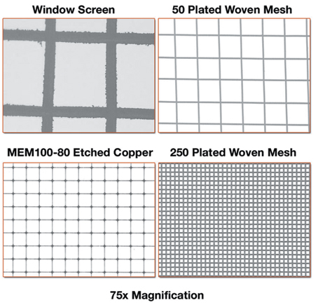
Fig. 4: For purposes of comparison, a typical window screen mesh (left) is shown alongside three different fine-wire plated woven and etched meshes, at right. All are shown at 75x magnification.
For highest shielding applications, the mesh must be conductively plated (e.g., silver conductive plating) to fuse the wire crossovers. The mesh can then be blackened with a conductive, corrosion-resistant plating to improve galvanic stability and optical performance (by reducing reflections). Patterned conductive grids are typically produced by depositing a conductive ink or etching a metalized coating on a substrate. Wire diameters can be produced as fine as 0.0005 in. and therefore provide a higher open area as compared to their woven equivalents. The surface resistance of the material typically drives the shielding effectiveness over the RF spectrum; the more conductive the material, the better the shielding effectiveness. Additionally, as the open area increases, the shielding effectiveness will be reduced. Figure 5 shows a typical touch-screen construction which can be configured with either thin-film coating or fine-conductive-grid options.
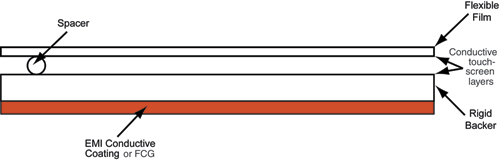
Fig. 5: Touch-screen constructions are shown with thin-film coating or fine-conductive-grid options.
Fine-conductive grids are typically specified by line pitch (e.g., the number of strands per inch in the x and y directions. For example, a mesh with 80 lines per inch in both the x and y directions would have lines spaced 0.0125 in. or 0.3175 mm and simply be called "80 mesh" for shorthand since the spacing is the same in both axes. Alternatively, it can be specified in terms of openings per inch (OPI). Standard mesh pitches range from 50 to 255 lines per inch (lpi). Different line pitches are available for increased shielding needs and for moiré control options. (See Table 2 for a comparison of transmittance, reflection, and shielding properties between coating and mesh technologies.)
Table 2: Thin-film conductive coatings and fine-wire mesh are compared in terms of transmittance, reflection, and shielding. Note: etched mesh with a wire width of 0.0005 in.
| CGP |
Transmittance (%)
|
Reflection (%)
|
Shielding
|
| 10-Ω/sq. Metal Alloy |
80
|
7 to 8
|
Low
|
| 10-Ω/sq. ITO |
88
|
7 to 8
|
Low
|
| 10-Ω/sq. IMITO |
≥ 96
|
< 0.5
|
Low
|
| 2-Ω/sq. ITO |
78
|
10
|
Fair
|
| 2-Ω/sq. IMITO |
≥ 87
|
< 1.0
|
Fair
|
| 50 Mesh |
80-85
|
0.15 to 0.35
|
Good
|
| 80 Mesh |
77-83
|
0.15 to 0.35
|
Good
|
| MEM100-80 |
81-86
|
< 0.6
|
Fair-Good
|
| 100 Mesh |
66-69
|
0.15 to 0.35
|
Good
|
| 255 Mesh |
40-44
|
0.15 to 0.35
|
Superior
|
EMI-shielding design
The EMI shield can be applied to the front or rear surfaces of the touch screen. Care must be taken not to interfere with the resolution or sensitivity of the touch screen if the touch screen itself must be shielded (i.e., the CGP is on the outermost surface). Thin-film conductive coatings applied to the rear surface of the touch screen offer a simple, cost-effective way to achieve EMI attenuation but they do not prevent susceptibility or radiation of the touch screen itself. The degree of index matching of the rear surface is dependent upon the contrast required or the amount of rear surface reflection that can be tolerated.
Grounding the conductive coating can readily be achieved by using an electrically conductive pressure-sensitive adhesive (PSA) and attaching the touch screen to a metal LCD frame, bezel, or housing to complete the Faraday cage. A conductive adhesive or gasket can also be used to terminate the CGP. Whenever two light-transmitting matrices are overlaid, there is a potential for a moiré pattern to be generated. If the spatial frequency of the matrix is close to that of the display's pixels, the resulting moiré pattern (Fig. 6) will hinder display readability. Therefore, a touch screen with a fine-grid CGP must be optically fitted, by adjusting the grid orientation, to the specific electronic display (e.g., LCD) to minimize or eliminate this phenomenon. EMI/ EMC performance will not change when the grid orientation is adjusted. The necessity of creating a good "optical fit" makes the remote design process more challenging compared to designing with transparent film processes. Empirical optical testing may be required.
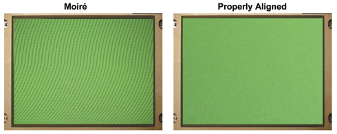
Fig. 6: The moiré effect is illustrated with incorrectly fitted (left) and properly optically fitted (right) fine-conductive grids.
Conclusion
Touch screens are becoming more and more prevalent as the user interface of choice for high-ambient-light readability applications. COTS touch screens can be optimized to improve both environmental and optical properties. Knowing that the performance of COTS touch screens can vary, it is best to start with a product that has properties close to those required in the end application and to select touch-screen attributes that will not interfere with any required enhancements. To minimize EMI in the final product, shielding enhancements can be readily incorporated into either the front or rear surface of the touch screen using a lamination process of secondary materials (although a conductive ground plane is more readily applied to the rear of the touch screen). Transparent thin-film conductive coatings are recommended for applications requiring low levels of EMI shielding, low package thickness, and low cost. Fine conductive grids are the material of choice for very high levels of shielding (Table 3).
Both technologies should be considered for moderate levels of shielding. Because there is not one solution that works best for all applications, each should be considered unique and the particular EMI enhancement should be selected for specific end-program suitability. •
Table 3: Design considerations involved in selecting a touch-screen optimization technology include cost, shielding needs, and appearance.
| Priority |
Recommended Designs |
| Cost |
Film |
| Shielding needs |
Conductive grids (woven and etched mesh) |
| Visual appearance |
Film (Film is continuous; all conductive grids present the possibility of moiré generation, and require optical fitting); Etched mesh (near-perfect uniformity) |
Brian Herr is Display Integration Manager, Jeff Blake is Director of Sales and Marketing, and Richard Paynton is President & CEO at Dontech, Inc., in Doylestown, PA. Jeff Blake can be reached via jblake@dontechinc.com.