| The Transition from Driving LED Backlights to Driving Solid-State Lighting
The secret to getting the most from LED solid-state lighting is to understand that different topologies must be implemented for different applications.
by Graham Upton, Michael Keene, and Michael Kretzmer
THE LIGHT-EMITTING DIODE (LED) has come a long way from its humble beginnings as a simple indicator light to the basis of the plethora of applications for which it is used today. Market analysis suggests that it is relatively early in the LED's development, and that as it continues to mature over the next few years, we will see numerous industries greatly transformed by the introduction of today's higher-efficacy, lower-cost LEDs. Those of us in the display industry have watched as LEDs slowly infiltrated some of the smaller display backlights and recently spread to the medium- and larger-sized LCDs.
As the LED is adopted into different mediums, special attention should be paid to the way in which LEDs are electrically controlled in order to maximize the total value of the design. Although great advances have been made in IC and LED driver design, there is no one-size-fits-all LED driver. Today's savviest designers and integrators let their application needs and functional requirements dictate the best type of driver to install in their application. Prior to selecting an LED driver for an original-equipment-manufacturer (OEM) display, for example, Endicott Research Group encourages integrators to prioritize the features that will influence the selection. Some of the key parameters include size, cost, efficiency, power, noise, dimming, and flexibility. Often the driver design will be partially dictated by decisions made higher up in the supply chain (for example, LED string configurations). This phenomenon is in no way unique to the display industry and factors into other areas of solid-state lighting (SSL). This article will highlight some of the standard topologies currently employed to drive OEM LED-backlit displays and move on to discuss some of the major hurdles that inhibit a generic LED driver from being implemented directly into general lighting.
AC/DC LED Drivers for SSL
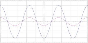
The International Electrotechnical Commission (IEC) and American National Standards Institute (ANSI) have defined requirements for power-factor and input-current harmonics generated by power supplies fed by AC line voltage. These requirements vary depending on application, and both agencies have specific requirements for lighting equipment. Power factor is defined as the ratio of real to apparent power being consumed by an electronic device, which speaks to the phase relationship between current drawn from the line and line voltage. When the input current consumed by an electronic device is linearly proportional to and in phase with the input voltage (as with a purely resistive load), the power factor is said to be unity (or 1) [Fig. 1(a)]. A power factor of unity is ideal because it reduces distribution losses and contributes little noise and distortion to the line.
When a load is composed of either non-linear or reactive circuit elements, the power factor deviates from unity. If a load is linear, capacitive, and resistive, the input current will lead the input voltage [Fig. 1(b)]. If a load is linear, inductive, and resistive, the input current will lag the input voltage. In either case, the apparent power (the instantaneous product of voltage and current) will not equal the actual power. One reason why agencies such as IEC and ANSI have imposed limits on the difference between real power and apparent power is that many power utility meters measure apparent power.
Bridge Rectifier and Bulk Capacitor in AC/DC Converters
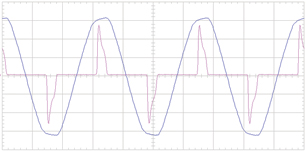
Before power factor and current harmonic limitations were adopted, the majority of single-phase power supplies consisted of a bridge rectifier and bulk capacitor, which would convert the incoming AC into DC with some ripple. That ripple would then be filtered out by additional passive filters or active regulators, creating smooth DC power. While this circuitry is inexpensive and simple to imple-ment (and still commonly used in low-wattage supplies today), the combination of bridge rectifier and bulk capacitor consumes nearly all of the input current during a brief period when the sinusoidal input voltage waveform is at its peak, creating a highly distorted input-current waveform [Fig. 1(c)]. The reason this brief current draw occurs is that the bridge rectifier is not forward-biased and conducting until the instantaneous line voltage exceeds the DC voltage across the bulk capacitor. (As stated, this current draw only occurs at the peak of the input voltage waveform.) Consequently, these input-current spikes reduce the efficiency of the power distribution network because the instantaneous power lost in the line is equal to the square of the input current multiplied by the line resistance. In addition to this reduction in efficiency, the line voltage becomes distorted near the peak of the sinusoidal waveform [notable in Figs. 1(c) and 1(d)] when the distribution network is excessively loaded with devices utilizing this configuration of AC/DC conversion. In order to control the current draw from the line, an active power-factor-correction (PFC) circuit may be used. Figure 1(d) shows the typical input current draw for an active PFC circuit.
Power-Factor-Correction Circuit
In order to reduce the input-current harmonics that the bridge rectifier and bulk capacitor AC/DC conversion circuit create, and to keep the current drawn by the power supply in phase with the input voltage, a circuit very similar to that shown in Fig. 2 can be utilized. This circuit, based upon a pulse-width-modulating (PWM) boost converter, is popular and well documented, although it is not the only currently utilized active PFC topology.
 (a) (a) 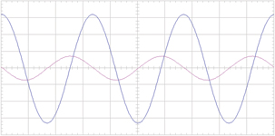 (b) (b)
 (c) (c) 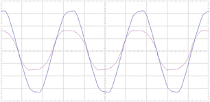 (d) (d)
Fig. 1: In charts (a)–(d), the input voltage is represented by the blue line and input current by the pink line. (a) Unity power factor. (b) Non-unity power factor. A 90° phase shift between input current and input voltage is the result of a capacitive load. (c) Input voltage and current waveforms typical of the bridge rectifier and bulk capacitor combination. (d) Typical input voltage and current waveforms for a PFC circuit.
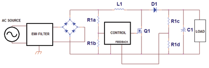
Fig. 2: This typical resistive network configuration shows the non-isolated PFC stage.
The main difference between a "boosting" PFC and the boost converter is that the PFC circuit modulates its input-current consumption in order to create an input-current waveform that approximates that of a resistive load. In Fig. 2, this input-current shaping is achieved by sampling the input voltage (in the U.S., a 120-Hz rectified version of the input voltage) and modulating Q1 on time so that the circuit consumes a nearly sinusoidal input current that matches the input voltage in frequency and phase. The resistive network seen in Fig. 2 is not always the scheme used for determining the correct modulation of input current, but is a popular one nonetheless. The main reason a boost converter is the basis of most active PFC circuits utilized today is that the boost can draw input current from the line from just above 0 V to the peak of the AC waveform, limiting input-current distortion.
PFC circuits generally require a large amount of output filtering capacitance (C1) because they pass a large amount of low frequency to the output when modulating the input current. These circuits also generate very high output voltages, typically 200–400 V or more (they can only boost the 110 or 220 V coming in!), requiring the addition of a conversion stage between the PFC output and the load circuitry. The high output voltage of the boost converter is not generally desired; it is merely a by-product of the architecture. In addition to the current-control circuitry an active PFC incorporates, nearly all switching converters connected to the line require a complex filter at their input to reduce the noise they generate back to the utility and to filter the noise coming off the line.
The Two-Stage Approach to AC/DC Conversion
The typical loads that an AC/DC converter driving a series string of LEDs will power often run on 48 V or less (nowhere near the 200 V a non-isolated PFC converter will output in many cases). Therefore, a DC/DC converter (usually one that isolates the output from the input via a transformer) generally follows the PFC and is used to convert the high-voltage output from the power-factor corrector to a voltage or current suitable to drive the load. The advantage of this configuration is that the converter driving the load directly is supplied with a mostly DC input voltage, allowing the supply to have high-input rejection and high-load regulation. If properly configured, the power stage is capable of driving multiple LED strings and providing an isolated output. One drawback to this configuration is that the losses from the PFC and DC/DC converter are in series, typically limiting the efficiency to the high 70% and low 80% range. Because LEDs are a disruptive technology for general lighting – and because expectations about the energy savings inherent in switching to SSL are so high – driving at a high efficiency is critical. This configuration also requires a significant number of components and board layout space for two power converters, which results in a large footprint and high cost.
A Single-Stage Approach to AC/DC Conversion
One way to limit power-supply footprint and part count is to change the configuration of the PFC from a boost to a flyback converter and to add a stage of isolation to the feedback network. This circuit (Fig. 3) achieves AC/DC conversion and enables the PFC stage to create an output voltage that is greater or less than the input voltage. The circuit also achieves output isolation, which is necessary in many general lighting applications. The flyback transformer (T2), in which power is transferred from line to load, operates nearly the same as the boosting inductor in Fig. 2, with current flowing in the primary during Q2 on-time and in the secondary during Q2 off-time. Considering input current, the main difference between the boost and flyback configuration is that the flyback circuit does not draw current when Q2 is off. The rest of the circuit operates in the same way as a non-isolated boost PFC. This configuration, if properly implemented, can achieve efficiencies in the high 80% to low 90% range and can reduce cost when compared with the two-stage approach. Poor line rejection and mediocre load regulation are inherent to this circuit's operation; therefore, it is only recommended for driving loads such as LEDs that are not highly susceptible to moderate ripple and voltage variations. This circuit forms the basis of a single-string current source, as well as a multiple-string current source, which will be discussed shortly.
Those with experience in driving LEDs know that it is not enough simply to have clean DC power because LEDs need to be driven by a constant-current source in order to avoid thermal runaway and other failure-mode effects. Indeed, the low-voltage output described above does require additional hardware to provide the constant current for the LEDs. Regardless of how it is labeled, this style of low-voltage output is a popular mode of powering LEDs be-cause it allows the integrator a great deal of flexibility with the load and reduces the number of different power supplies that have to be stocked. For example, a lighting designer may configure from 1 to 11 strings of up to 6 or 7 LEDs to a single 100-W 24-V single-output power supply. Of course, each string requires a constant-current provider. The alternate method is to use a power supply that includes a constant-current source onboard, but one is needed for each string of LEDs that must be driven. Both methods have several advantages and disadvantages, as shown in Table 1.
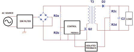
Fig. 3: This PFC incorporates isolated output.
Power-Factor-Correction Circuit with Current Output
With a simple modification that converts the output-voltage feedback network to an output-current feedback network, the power-factor- correction circuit shown in Fig. 3 will maintain a constant output current as opposed to a constant output voltage. This change in the feedback configuration is identical to that between the PWM voltage boost and PWM current boost (both driven by DC as opposed to AC sources, and neither requiring output isolation). As with the PWM boost, this circuit will only drive one LED string. As discussed for the previous circuit, the single-stage approach will not achieve the input rejection or load regulation that the two-stage approach is capable of, but because an LED string is a static, moderately insensitive load, only marginal output regulation is required. Because calling an LED load "moderately insensitive" is a qualitative assessment, it is necessary to note that LEDs do not require an extremely low ripple supply to create a uniform and consistent perceived brightness. Moderate PWM dimming ratios are achievable, although LED current-amplitude modulation as opposed to PWM may be required in many situations. The drawbacks of PWM dimming are currently the subject of debate among many engineering and also healthcare professionals. Dimming via PWM requires that all dimming circuits be locked together (or synchronous) in frequency; otherwise, beat frequencies, or perceivable "flicker," can occur. When dimming is synchronous, the frequency must be high enough that the human eye does not perceive any "strobing" (the human eye can perceive frequencies well above 120 Hz in some cases). This "strobing" can create health issues for those with epilepsy and also pose a hazard for oper-ators of heavy machinery in industrial environ-ments where the perception of motion is key.
The Linear Current Source
Linear current sources are the most widely used current sources in low-power applications (including many OEM LED displays) due to their small size and lack of a costly magnetic component. Linear current sources are relatively easy to implement and many fully integrated adjustable voltage regulators can be easily configured as a linear current source. While there are many different linear-current-source topologies, one of the most widely used is seen in Fig. 4. This circuit is the design upon which many popular IC voltage and current regulators are based. U3 acts as the "brains" of the circuit, continuously comparing the amount of current flow through the load to a reference level and making adjustments (via Q3) if necessary. The main advantage of a linear current source is the low parts count, low cost, and relatively small size. The main disadvantage to linear current sources is that they require greater headroom (and therefore dissipate more power) than switching current sources, such as the hysteretic and PWM current sources. This power dissipation inherent to linear current sources limits them to lower power applications or applications that can tolerate large heat sinks and higher device junction temperatures.
|