Emerging Technologies for the Commercialization of AMOLED TVs
Advances in AMOLED materials, device structures, and manufacturing are paving the way for a new generation of TVs that will be interactive, ultra-light and slim, eco-friendly, and more.
by Hye Dong Kim, Hyun-Joong Chung, Brian H. Berkeley, and Sang Soo Kim
<!--preview-->
SINCE THE FIRST market emergence of black-and-white CRT TV in 1937, the evolution of TV technology has accelerated with increasing demands for better picture quality and realistic image reproduction. It took more than 30 years for color TV to replace black-and-white CRT TV. Then 20 years later, demands for larger and flatter screens resulted in flat CRT and projection TV being introduced to the market. About 15 years later, the high-end market was revolutionized with the launch of flat-panel displays based on plasma and liquid crystals. In particular, LCD technology, which dominates the TV market these days, is further evolving with the adoption of high-speed driving and LED backlights that enable slim TVs with low power consumption.
Active-matrix organic light-emitting diodes (AMOLEDs) are ideally suited for future TV applications because of their superb image quality, digital addressing, and self-emissive nature. AMOLEDs are rapidly expanding their market share for small-sized mobile applications since their mass production launch in 2007. In addition, exhibitions of Sony's 27-in.1 and Samsung's 31-in.2 and 40-in.3AMOLED TV prototypes have resulted in massive "wow factor" recognition from experts and the public.
In this article, we will review the tech-nological challenges with regard to mass commercialization of AMOLED TVs, as well as the emerging technologies that will overcome these challenges.
AMOLED: The Ultimate Solution for Future TV
The basic and most important feature of TV is the ability to faithfully reproduce real images. With the launch of high-definition digital broadcasting, viewers can now enjoy a vivid presence from large flat-panel-TV screens. As a result, perceptual image quality, which is the reproduction of real color and motion features, has become more important than measures such as contrast, luminance, and color gamut. Because AMOLEDs are self-emitting, light emission can be controlled for each pixel at extremely high speed. Therefore, AMOLEDs are intrinsically capable of expressing high contrast, blur-free motion features, vivid colors, and wide viewing angle. Old color-gamut models cannot express these perceptual image qualities; thus, new standards, such as CIECAM02, the most recent color appearance model ratified by the C.I.E. (http://www.cie.co.at/index_ie.html), have been suggested. Figure 1 compares the perceptual image qualities of OLEDs and LCDs. AMOLEDs can produce more vivid images at low brightness due to their high contrast ratio and peak luminance. These advantages result from the deep-black background and self-emitting nature of OLEDs.
The global environmental crisis has gained attention recently, and for geopolitical and economic reasons, many countries are legislating green policies. Naturally, TVs are also required to be eco-friendly. The environ-mental compatibility of flat-panel displays can be categorized into each of the areas of components, manufacturing processes, and power consumption. AMOLEDs offer advantages in each of these areas.
From a component point of view, AMOLEDs are intrinsically eco-friendly because they do not contain backlights or color filters and do not require many other optical components. Removal of the backlight provides the additional advantage of a slimmer and more light-weight panel, creating a more eco-friendly product as a result of reduced energy consumption for transportation. In addition, AMOLED panel components are free from toxic materials, such as Hg and Cd, whose application is prohibited by RoHS regulations.
For the manufacturing process, the key to eco-friendliness lies in minimal production of waste by-products. For example, wet-etch and spin-coating processes waste large amounts of chemicals, whereas ink-jet printing results in good material usage efficiency. OLEDs are advantageous from an environmental point of view because their manufacture makes use of direct-patterning processes such as shadow masks and printing.
In terms of power consumption, AMOLEDs have a great advantage over LCDs built with "always-on" CCFL or edge-lit-LED backlights. In an AMOLED, each pixel is individually controlled, and light is only generated if it is actually needed for the display. Furthermore, there is still significant opportunity for further reduction in AMOLED power consumption. For example, phosphorescent light-emitting materials represent an exciting recent development in OLED technology. If phosphorescent emitters can replace current fluorescent emitters, an extremely power efficient (<15 W) 40-in. TV could be possible by 2012, according to Universal Display Corp. (Fig. 2).
Technological Challenges for AMOLED TV
In recent exhibitions, Sony and Samsung displayed the potential of AMOLED TV by making the largest size possible on their pilot lines (27-in. for 3G and 40-in. for 4G, respectively). For mass production, however, AMOLED TVs must be manufactured at a cost that competes with LCD TVs. Current AMOLED mass-production lines employ an excimer-laser-annealing (ELA) based poly-Si TFT backplane, a shadow mask for color patterning, and edge sealing for encapsulation on a 3.5G-sized (460 mm x 730 mm) motherglass.
The biggest hurdle for commercially viable large-sized AMOLED TV is the need to increase the motherglass size. In order to compete with the cost of LCD TVs, multiple panels must be fabricated on a single motherglass, and 8G (2200 mm x 2500 mm) or larger glass is desired. Existing mass-production technologies, however, face limitations in scaling up to this size; therefore, new methods are required.
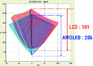
Fig. 1: Perceptual contrast-length comparison of LCDs and AMOLEDs expressed on CIECAM02 color space. The luminance values of LCDs and AMOLEDs are 256.3 and 189.9 cd/m2, respectively. It is notable that only 110.9 cd/m2 is required for AMOLEDs to achieve the same perceptual contrast length as LCDs. Source: Samsung.
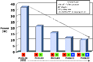
Fig. 2: Above is a power-consumption roadmap for a 40-in. AMOLED panel based on expanded incorporation of phosphorescent OLED (PHOLED) technology over approximately 5 years. Source: Universal Display Corp.
Emerging Backplane Technologies
OLEDs are current-driven devices, which places additional requirements on the backplane, including precise control of current and high-threshold-voltage stability. Low-temperature poly-Si (LTPS) TFT backplanes fabricated by ELA are currently employed in the mass production of AMOLEDs, owing to their excellent TFT performance and device stability. However, uniformity and scalability issues create challenges for the use of ELA in large-area applications. For example, laser-power fluctuation can cause image non-uniformity, and a finite laser-beam length restricts process scalability. Moreover, ELA-based LTPS TFTs require many (8–11) masks compared to the number of masks required for LCDs (4); thus, ELA-based LTPS is less cost-effective and less eco-friendly.
Because laser equipment is expensive and can present maintenance problems, generally, non-laser crystallization techniques are believed to have greater potential for large-sized AMOLEDs. One of the simplest non-laser methods to increase mobility of amorphous-Si (a-Si) film is conventional solid-phase crystallization (SPC). But SPC usually requires high-temperature (>650°C) annealing for a relatively long time, and thus can be harmful for large-area glass substrates. One way to reduce the crystallization temperature is to apply metal atoms as crystallizing seeds on the a-Si surface. However, these metal seeds can contaminate the channel area and thus may result in large current leakage. Moreover, the grain size from this method is usually small and irregular, resulting in lower mobility and high grain-boundary-induced leakage current. In order to circumvent these drawbacks, the super grain silicon (SGS) method has been suggested.4 SGS employs a sacrificial capping layer on the a-Si layer before seeding metal deposition, followed by annealing to diffuse metal atoms to the a-Si surface through the capping layer. However, the application of SGS is challenged by its complicated process and production yield.
Amorphous-oxide TFTs have great potential to scale up size. Basically, oxide TFTs combine the merits of a-Si and LTPS TFTs.5 For example, oxide TFTs are free from the non-uniformity problem that comes from the polycrystalline nature of LTPS, while their device performance is reasonably good with large carrier mobility (~10 cm2/V-sec) and excellent sub-threshold gate swing (down to 0.20 V/dec). Moreover, the channel layer can be formed by a simple sputtering process without further crystallization steps; thus, the fabrication process can basically be identical to that of a-Si TFTs for LCDs. For this reason, existing a-Si production lines can easily be converted without significant change. In addition, oxide TFTs can be deposited at room temperature; thus, cheap soda-lime glass or flexible plastic substrates can be used in principle. However, device instability issues need to be addressed in order for oxide TFTs to be used for AMOLEDs. As is well known, oxide semiconductors are sensitive to oxygen and moisture, and for this reason they have long been used as sensor materials. Therefore, environmental control during the production process and proper passivation techniques are required for oxide TFT fabrication.
Emerging OLED Patterning Technologies
Shadow-mask technology, also known as fine metal mask (FMM), is currently being employed in the mass production of AMOLEDs. However, FMMs are prone to sagging problems when applied to large-sized motherglass because the masks are made by metal films that are too thin (50 μm) to be used over a large area. In addition, FMMs have other issues such as pixel-size variation by ±10 μm, shadow effects due to non-zero metal thickness, and alignment accuracy between the mask and substrate. Frequent mask cleaning is also required to maintain pattern quality. An alternative solution could be to use white OLEDs with color filters. However, the white-OLED approach sacrifices some of the advantages that come from the self-emissive nature of OLEDs; thus, this approach is not an optimized solution for large AMOLEDs. For this reason, emerging OLED patterning technologies, including ink-jet printing, nozzle printing, and laser-induced printing, are receiving a great deal of attention for potential application to large AMOLEDs (Fig. 3).
Among the laser-induced printing techniques, laser-induced thermal imaging (LITI),6 radiation-induced sublimation transfer (RIST),7and laser-induced pattern-wise sublimation (LIPS)8 are currently under development for mass production. These technologies are in principle very similar in the sense that the patterns are transferred from a donor substrate to the active-matrix backplane by local heating using laser beams. The major difference is that LITI transfers the OLED layer from a conformable donor film by local melting, whereas RIST and LIPS use a glass donor substrate and the transfer occurs by sublimation of materials while the gap between the donor and the active-matrix backplane is in vacuum. Current issues from these laser technologies are thermal damage, process stability, and process yield.
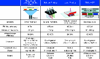
Fig. 3: AMOLED color patterning technologies include evaporation, solution printing, laser printing, and white and color filters.
Direct-printing methods, such as ink-jet and nozzle printing, use solution-based OLED materials. These approaches have the potential to be the most cost-effective and eco-friendly because they exploit complete use of the OLED materials. However, solution-based OLED materials are often very expensive. Compared to evaporation-based materials, solution-based materials face a serious disadvantage, which is that OLED lifetime is extremely sensitive to impurities, film quality, and environmental conditions. The development of high-performance soluble OLED materials is the biggest challenge for the use of printing for OLED patterning.
Encapsulation Issues
For reliable operation and long-term performance, OLEDs must be encapsulated. For small-sized AMOLED devices, edge-sealing encapsulation is adequate for the fabrication of reliable panels. However, for large devices, edge sealing has some serious problems, including delamination, sagging, and breaking of the encapsulation glass by external stress. In order to prevent breakage and to improve mechanical reliability, new techniques are currently under development, including filling the gap between the AMOLED and encapsulation glass and the use of non-etched glass. Challenges for these techniques include the development of liquid filler material and film-lamination technology.
Thin-film encapsulation (TFE) can provide another interesting solution for large-area encapsulation.9 Instead of using encapsulation glass, TFE employs layer-by-layer deposition of thick films with compensating diffusion barrier properties. The biggest merit of TFE is that it enables a single glass display, in turn enabling extremely slim and flexible panels. Challenges for TFE include material optimization, minimization of stacking layers, and applicability to large-sized motherglass.
Circuit Issues
In AMOLEDs, the active-matrix circuit lies beneath each pixel, and the circuit is comprised of power-supply lines and power-control TFTs. For each AMOLED pixel, at least two transistors (switching and driving) and one capacitor are required. However, because the OLED pixel luminance is directly changed by the current, subtle variations in the TFT current result in brightness differences from pixel to pixel. As a result, even a slight non-uniformity in TFT performance can create serious image-quality problems. For this reason, most AMOLED panels incorporate compensation circuits to correct this problem.
Two types of compensation circuits, current programming and voltage programming, have been suggested. The-current programming method compensates TFT threshold-voltage and mobility differences, whereas voltage programming compensates only for the threshold-voltage differences.10, 11 However, for large-area applications such as TV, the voltage-programming method is more useful because of its ability to work over large areas and for compatibility with LCD driver ICs.
AMOLED Prototypes Utilizing Emerging Backplane Technologies
Samsung has demonstrated a 40-in. AMOLED TV prototype by combining an SGS-based LTPS TFT backplane and FMM OLED technologies.3 A 12-in. AMOLED notebook panel has also been prototyped and exhibited by the use of amorphous-oxide TFT backplanes and FMM OLED technologies.12 Figure 4 shows images and specifications of these demonstration panels.
Conclusion
Due to fundamental advantages in display quality, underlying cost, and eco-friendliness, we believe a new era of AMOLED TV is inevitable. In this article, technological challenges have been discussed from the point of view of the active-matrix backplane, OLED patterning, and encapsulation processes. In order to effectively compete with LCDs, AMOLEDs need to realize their full potential both in terms of eco-friendliness and price competitiveness. The best future AMOLED-TV solution may incorporate a combination of a-Si TFT-like backplane, printing-based OLED patterning, and thin-film encapsulation technologies.
AMOLEDs are ideally suited to become the TV of the future – not only due to their superb image quality and eco-friendliness, but also based on their potential to expand the scope of displays. Indeed, the use of AMOLEDs has already resulted in real displays, including transparent, bendable, foldable, and flexible displays that were previously only conceived of in science-fiction movies. As convergence technology and interactive interfaces become increasingly important, the need for vivid and intuitive displays will certainly grow, and these changes will transform the concept and expectation of future TVs. AMOLEDs provide special capabilities and will inspire completely new applications that are not yet conceived, thus revolutionizing the future TV industry.
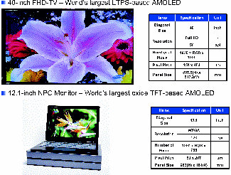
Fig. 4: 40-in. full HD and 12.1-in. WXGA AMOLED displays have been displayed by Samsung.
References
1Exhibited at CES in 2007.
2Exhibited at CES in 2008.
3Exhibited at FPD International in 2008.
4H.K. Chung and K.Y. Lee, SID Symposium Digest 36, 956-959 (2005).
5J. K. Jeong, J. H. Jeong, J. H. Choi, J. S. Im, S. H. Kim, H. W. Yang, K. N. Kang, K. S. Kim, T. K. Ahn, H.-J. Chung, M. Kim, B. S. Gu, J.-S. Park, Y.-G. Mo, H. D. Kim, and H. K. Chung, SID Symposium Digest 39, 1–4 (2008).
5S.T. Lee, M.C. Suh, T.M. Kang, Y.G. Kwon, J.H. Lee, H.D. Kim, and H.K. Chung, SID Symposium Digest 38, 1588-1591 (2007).
6M. Boroson, L. Tutt, K. Nguyen, D. Preuss, M. Culver, and G. Phelan, SID Symposium Digest 36, 972-975 (2005).
7T. Hirano, K. Matsuo, K. Kohinata, K. Hanawa, T. Matsumi, E. Matsuda, R. Matsuura, T. Ishibashi, A. Yoshida, and T. Sasaoka, SID Symposium Digest 38, 1595-1595 (2007).
8A. B. Chwang, M. A. Rothman, S. Y. Mao, R. H. Hewitt, M. S. Weaver, J. A. Silvernail, K Rajan, M. Hack, J. J. Brown, X. Chu, L. Moro, T. Krajewski, and N. Rutherford, SID Symposium Digest 34, 868-871 (2003).
9Y. Matsueda, D. Y. Shin, K. N. Kim, D. H. Ryu, B. Y. Chung, H. K. Kim, H. K. Chung, O. K. Kwon, IDW '04 Digest, 263-266 (2004).
10N. Komiya, C. Y. Oh, K. M. Eom, J. T. Jeong, H. K. Chung, S. M. Choi, and O. K. Kwon, IDW '03 Digest, 275-278 (2003).
11Exhibited at SID 2008. •
The authors are with the OLED R&D Center, Samsung Mobile Display Co., Ltd., San #24 Nongseo-Dong, Kiheung-gu, Yongin-si, Gyeonggi-do 446-711, Korea.