Emerging LCDs Based on the Kerr Effect
Liquid-crystal displays based on the Kerr effect have recently been drawing attention due to their fast response time and simple fabrication process. Understanding the device physics through numerical modeling of this emerging LCD technology will play an important role in improving display performance as well as optimizing configurations.
by Linghui Rao, Zhibing Ge, Sebastian Gauza, Shin-Tson Wu, and Seung Hee Lee
THE Kerr effect, first discovered in 1875, is a type of quadratic electro-optic effect caused by an electrical-field-induced ordering of polar molecules in an optically transparent and isotropic medium. Liquid-crystal displays (LCDs) based on the Kerr effect are now emerging because they exhibit the following three distinct advantages: (1) the fabrication process is simple and cost-effective because it does not require any alignment layers, (2) the voltage off-state is optically isotropic, which means that the viewing angle is wide and symmetric, and (3) the switching time is in the sub-millisecond range. Therefore, the technology can be used for color-sequential displays without the use of color filters, resulting in a 3X higher optical efficiency and resolution – provided that RGB light-emitting diodes (LEDs) are used for the backlight.
Background
Some isotropic transparent substances, such as liquids and glasses, can become birefringent when placed in an electric field E.1,2The Kerr effect differs from the Pockels effect (which occurs only in crystals that lack inversion symmetry, such as lithium niobate or gallium arsenide) in that the induced birefringence (Δn) from the Kerr effect is proportional to the square of the electric field instead of varying linearly. Because Δn cannot increase unlimitedly with the electric field, it can be written as1–3
Δn = λKE2 = (Δn)o(E/Es)2, (1)
where λ is the wavelength, K is the Kerr constant, E is the applied electric field, (Δn)o is the maximum induced birefringence, and the induced Δn saturates at (Δn)o when the electric field E exceeds a saturation field Es.
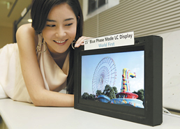
Fig. 1: Samsung's 15-in. blue-phase LCD prototypes were shown at Display Week 2008 (left) and 2009 (right).
Recently, this square-law-dependence phenomenon has also been observed in liquid crystals (LCs), such as polymer-stabilized blue-phase (BP) LCs. Moreover, amazingly, its Kerr constant is ~5–6 orders of magnitude higher than that of CS2. (The Kerr effect constant is on the order of 1 x 10-14 m/V2). BP is a type of LC phase that appears in a very narrow temperature range (1–2°C), between the chiral-nematic and isotropic phases, with a molecular structure comprising double-twisted cylinders arranged in a cubic lattice with periods of several hundred nano-meters.4,5 However, polymer-stabilized BP exhibits a fairly wide temperature range, including room temperature. As a result, novel LCDs based on the Kerr effect are possible; i.e., displays in which the birefringence is induced by the electric field rather than from the intrinsic Δn of the LC.
Samsung unveiled the world's first polymer-stabilized BPLCD prototype at the Display Week 2008 exhibition, arousing awareness in the display field that a technological revolution could be emerging. With its fast response time, this BPLCD can offer more-natural- appearing moving imagery with an unprecedented image-driving speed of 240 Hz (Fig. 1) or faster.
However, with this type of novel LCD based on the Kerr effect, the operating voltage is still too high (>50 Vrms) to be addressed effectively by conventional amorphous thin-film transistors (TFTs), due to a fairly small Kerr constant of the nano LC composite (K~1–10 nm/V2).6,7 Besides, the optical efficiency of the LC device is only ~65–75%. Therefore, there is an urgent need to develop material and device concepts to overcome these problems.
Approaches to Challenges
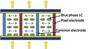
The authors have recently developed a model3,8 to simulate the electro-optical properties of LCDs based on the Kerr effect in in-plane-switching (IPS)9 and fringe-field-switching (FFS) cells.10 To achieve a high contrast ratio, a LC cell is sandwiched between two crossed linear polarizers. Without an applied voltage, the LC unit is optically isotropic, having identical refractive indices in its principal coordinates, which leads to a very good dark state. When a voltage is present, a strong electric field (E) from the IPS electrodes induces birefringence of the BPLC which changes the phase retardation of the incident light. The refractive ellipsoid will have its major optic axis aligned along the direction of the E vector.
Therefore, it is possible to first compute the potential distribution φ from solving the Poisson equation ∇(∇×εφ) = 0 and then the distribution of electric field E in the media. Based on the electric field, we further calculate the induced birefringence distribution Δnfrom Eq. (1) and assign the local optic-axis direction of each unit along the E vector. We confine the calculated birefringence from Eq. (1) to be below the intrinsic birefringence (Δn)o of the LC composite, and then compute, using an extended Jones matrix, the related electro-optical properties,11 such as voltage-dependent transmittance and viewing angle. Therefore, the dependence of LC electro-optics on different parameters such as wavelength, electrode configuration, and cell gap can be explored, as well as potential approaches for reducing the driving voltage.
The LC birefringence (Δn)o relates to the wavelength through the following single-band model12,13:
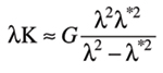 (2)
(2)
Here, λ* is the mean resonance wavelength and G is a proportionality constant. In an experiment with an LC cell based on the Kerr effect in the FFS structure by Ge et al.,3 researchers derived G ~ 8.78 x 10⁻³ V-2 for K ~ 1.27 nm/V2 at λ = 550 nm. Recently, H. Kikuchi's research group at Kyushu University in Fukuoka, Japan, reported a K ~ 10 nm/V2 at λ = 633 nm.7 Correspondingly, the authors have arrived at G ~ 8.78 x 10⁻² V-2 and K ~ 12.7 nm/V2 at λ = 550 nm. Together with λ* ~ 250 nm for E-7 type LC mixtures (Δn ~ 0.22) due to elongated π-electron conjugation,12 we can calculate, by using Eq. (2), the Kerr constants for λ = 450, 550, and 650 nm to be K ~ 17.6, ~ 12.7, and ~ 9.9 nm/V2, respectively.
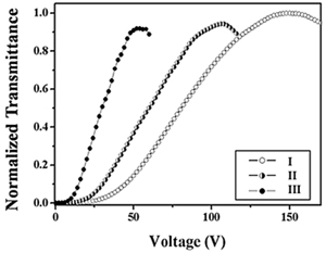
Figure 2 shows the simulated V–T curves of a 10-μm IPS cell with electrode width W = 5 μm and spacing L =10 μm. The electrode strips are placed at 45o with respect to the transmission axis of the top linear polarizer. The transmittance in the plot is normalized to the maximum value from two parallel polarizers at each wavelength. The color dispersion for red, green, and blue is comparatively larger than that of the nematic IPS or FFS cell. In a conventional nematic IPS or FFS cell, the on-state LC profile consists of two connected TN cells with a reversed twist sense; thus, this special two-TN-cell profile generates a self-compensation effect for wavelength dispersion.14 But in the IPS BPLC cell, the transmittance originates from the pure phase retardation of the Kerr effect, similar to a vertical-alignment (VA) cell. A shorter wavelength has a larger K constant and then a larger Δn/λ value; thus, the on-state voltage is lower. However, as opposed to the nematic VA cell, the induced birefringence (bright state) has a multi-domain structure originating from the electrical-field profiles. In an IPS cell, horizontal fields dominate between electrode gaps, while vertical components flourish above the electrode surfaces.14 Because each locally induced birefringence also aligns with the electric field, the induced refractive ellipsoids in the whole cell will gradually align from a vertical to a horizontal direction starting from the electrode center to the electrode gap. This multi-domain profile leads to a more symmetric and wider viewing angle, as will be shown later.
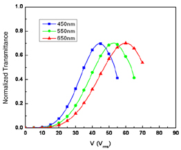
Fig. 2: The graph shows the V–T curves of the BPLC in an IPS cell with cell gap d = 10 μm, electrode width W = 5 μm, and spacing L = 10 μm at R (650 nm), G (550 nm), and B (450 nm) wavelengths. Kerr constant K=12.7 nm/V2 at 550 nm.
As for the electrode effect, the induced birefringence Δn from Eq. (1) is proportional to E2 and the optic axis of the ellipsoid is along the electrical-field vector E. In an IPS structure, the electric field is horizontal between the pixel and common electrode and vertical above the electrodes. For the LC cell at 45o away from the polarizer's transmission axis, only the induced Δn from the horizontal electric fields contribute to the overall transmittance; i.e., the high transmittance occurs between the electrodes. The incident light on top of the electrodes does not have any phase change because the optic axis of the refractive ellipsoid there is vertically aligned by the electric field. In a conventional nematic IPS cell, because the LC is a continuum material, the horizontal rotation of LC directors in the spacing area of the pixel and common electrodes will also produce a weak in-plane LC rotation on top of the electrodes and thus contribute to a weak light transmission, which eventually enhances the overall transmittance. However, in the IPS cell based on the Kerr effect, the viewing angle is more symmetric because the induced Δn above the electrode surfaces will act on the oblique incident light.
When it comes to the cell configurations in the electro-optics of the LCDs based on the Kerr effect, Fig. 3 shows the simulated V–Tcurves for cells in different W/L ratios (electrode width W to spacing width L), cell gaps, and Kerr constants (K1 = 12.7 nm/V2 and K2= 10K1). Generally speaking, the cell gap affects the transmittance and response time in a conventional IPS cell. However, the transmittance does not significantly change with cell-gap variance, as we can see from the V–T curves for the electrode dimensions (W = 5 μm, L = 10 μm) and (W = 5 μm, L = 5 μm) with cell gap d = 5 and 10 μm. This is because the penetration layer thickness for the induced Δn > 0.05 at the spacing area is only ~0.1–0.2 μm.8 As we know, the transmittance mainly comes from the contribution of the induced birefringence from the Kerr effect in the spacing area in between the electrodes. As long as the cell gap is larger than the fairly small penetrating depth in the vertical direction, the transmittance would not critically depend on the cell gap. The tiny shift may come from a passivation layer with a much smaller dielectric constant than the LC composite, which makes the electric energy more concentrated in the LC layer in a 5-μm cell rather than a 10-μm cell. For the electrode dimensions, a smaller electrode spacing usually leads to a stronger electrical-field intensity, which in turn results in a lower driving voltage. For example, in Fig. 3, the operating voltages of electrode configuration (W = 5 μm, L = 5 μm) are always lower than that of the dimension (W = 5 μm, L = 10 μm). Considering that only the regions between electrodes contribute to the transmittance, a larger L/W ratio favors the dimensions of (W = 5 μm, L = 10 μm) and (W = 2 μm, L = 4 μm) with L/W = 2 having higher transmittance than the dimension (W = 5 μm, L = 5 μm) with L/W = 1. However, the IPS cell with W = 2 μm and L = 4 μm exhibits a slightly higher operating voltage as compared to the cell with W = 5 μm and L = 5 μm. In an IPS cell, the electric fields generated from the bottom in-plane electrodes penetrate into the LC layer with a depth proportional to W + L, which is typical for a Poisson problem in the form of ∇2Φ = 0. As a result, for two IPS cells with a similar electrode spacing width L, the one with a larger dimension (W + L) will have a thicker LC penetrating depth contributing to the induced Δn and thus a lower voltage is needed for the peak transmittance. If we compare the V–T curves of (W = 2 μm, L = 4 μm) at K1 = 12.7 nm/V2 and K2 = 10K1, the on-state voltage drops from ~40 Vrms at K = K1 to ~ 12.5 Vrms by ~3.2X at K = 10K1. According to Eq. (1), we can estimate the operating voltage from the following relation: 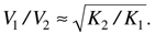 To reduce the driving voltage, an LC material with a higher Kerr constant, birefringence, and dielectric anisotropy would be a good choice.
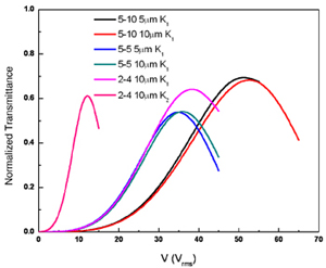
Fig. 3: Shown are V–T curves with different electrode dimensions and Kerr constants at λ = 550 nm of the IPS LC cells based on the Kerr effect (K1=12.7 nm/V2 and K2=10K1).
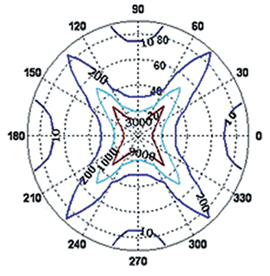
The viewing angle of LCDs based on the Kerr effect is wide and symmetric. In the dark state, when no voltage is applied, the LC behaves like an optically isotropic material. Therefore, the light leakage occurs only at an off-axis inci-dence when two crossed linear polarizers appear to no longer be perpendicular to each other. For an on-state voltage, a multi-domain-like Δn profile is induced due to the electrical-field distribution in an IPS cell. Therefore, the iso-brightness contour of the cell is very symmet-ric, as shown in Fig. 4, for an IPS cell with strip electrodes (width W = 5 μm and spacing L = 10 μm) at λ = 550 nm. To compensate for the viewing angle, both uniaxial films and biaxial films can be employed to reduce light leakage in the dark state and to expand the viewing angle.15 A contrast ratio of over 500:1 can be easily achieved for over 70°, as shown in Fig. 4(b), which is comparable to that of a conventional four-domain IPS structure.
To address the high-driving-voltage problem, some experts have also proposed a partitioned, wall-shaped electrode device structure driven with two TFTs to generate strong in-plane electric fields throughout the LC layer.16 The ideal cell configuration is shown in Fig. 5(a). With this structure, the electric field intensity E remains the same throughout all the vertical positions of the LC layer. As a result, the uniformly distributed horizontal electric fields help reduce the required operating voltage significantly. LC cells in conventional LCDs are usually driven by AC voltage to eliminate image sticking. The conventional 1TFT driving scheme fixes the voltage of common electrodes at a certain value; e.g., Von, and then signals a change in the voltage of the pixel electrode from 0 to 2Von in the dot-inversion driving scheme. Thus, the maximum possiblevoltage that can be applied to an LC cell (at Von) is reduced to half of the TFT driver capability (2Von). The proposed 2TFT driving method allows a separate control of pixel and common electrodes to maximize the possible driving capability of the IC driver. For example, when the potential of the TFT for pixel electrode is Von (0 V), the corresponding voltage on the common electrode can be 0 V (Von) to generate +Von (–Von). In Fig. 5(b), the cell parameters are electrode width W = 5 μm, electrode gap L = 10 μm, and cell gap d = 10 μm (K = 7 nm/V2). By simulating and comparing the results of (i) the conventional IPS device, (ii) the proposed device using partitioned wall-shaped electrodes with 1TFT driving, and (iii) the proposed device with 2TFT driving, the proposed structure (iii) shows an ~2.8x improve-ment in effectively reducing the operating voltage than the conventional IPS structure.
Thus far, we have investigated the device physics and analyzed, in detail, the LC electro-optics by numerical modeling. By using the correct concept, device structures can be optimized to reduce the operating voltage and further enhance the optical efficiency, just like the proposed partitioned wall-shaped electrode structure driven with 2TFT driving. On the other hand, employing a LC mixture with a larger Kerr constant is increasingly popular because the required electric-field intensity decreases as the Kerr constant rises.
 (a)
(a)
 (b)
(b)
Fig. 4: Simulated isocontrast plots appear (a) without any compensation film and (b) with a biaxial film with Nz =0.5, R0 = (nx-ny)d = l/2. Cell configurations: d = 10 μm, W = 5 μm, L=10 μm, K=12.7 nm/V2 at 550 nm.
LCDs based on the Kerr effect are attractive because of their fast switching time, very symmetric viewing angle, and ease of fabrication process without the need for alignment layers. If the challenges involving high voltage and low efficiency can be properly addressed, a new era of LCDs could be upon us.
References
1E. Hecht, Optics, 4th edition (Addison Wesley, 2002).
2A. Yariv and P. Yeh, Optical Waves in Crystal: Propagation and Control of Laser Retardation (Wiley, Hoboken, 2002).
3Z. Ge, S. Gauza, M. Jiao, H. Xianyu, and S. T. Wu, Appl. Phys. Lett. 94, 101104 (2009).
4S. Meiboom, J. P. Sethna, W. P. Anderson, and W. F. Brinkman, Phys. Rev. Lett. 46, 1216 (1981).
5R. Memmer, Liq. Cryst. 27, 533 (2000).
6S. W. Choi, S. Yamamoto, Y. Haseba, H. Higuchi, and H. Kikuchi, Appl. Phys. Lett. 92, 043119 (2008).
7H. Kikuchi, Y. Haseba, S Yamamoto, T. Iwata, and H. Higuchi, SID Symposium Digest 39, 579 (2009).
8Z. Ge, L. Rao , S. Gauza, and S. T. Wu, J. Display Technol. 5, 250 (2009).
9M. Ohe and K. Kondo, Appl. Phys. Lett. 67, 3895 (1995).
10S. H. Lee, S. L. Lee, and H. Y. Kim, Appl. Phys. Lett. 73, 2881 (1998).
11Z. Ge, T. X. Wu, X. Zhu, and S. T. Wu, J. Opt. Soc. Amer. A. 22, 966 (2005).
12S. T. Wu, Phys. Rev. A. 33, 1270 (1986).
13S. T. Wu, C. S. Wu, M. Warenghem, and M. Ismaili, Opt. Eng. 32, 1775 (1993).
14Z. Ge, S. T. Wu, S. S. Kim, J. W. Park, and S. H. Lee, Appl. Phy. Lett. 92, 181109 (2008).
15X. Zhu, Z. Ge, and S. T. Wu, J. Display Technol. 2, 2 (2006).
16M. S. Kim, M. Kim, J. H. Jung, K. S. Ha, S. Yoon, E. G. Song, A. K. Srivastava, S. W. Choi, G. D. Lee, and S. H. Lee, SID Symposium Digest 40, 1615 (2009). •
 (a)
(a)
(b)
Fig. 5: At left, (a) shows a cross-section in which the glass substrates are connected (spaced apart) by conducting walls; red for pixel electrodes and blue for common electrodes. (b) shows (i) the conventional IPS device, (ii) the proposed device using partitioned wall-shaped electrodes with 1TFT driving, and (iii) the proposed device with 2TFT driving.
L. Rao, S. Gauza, and S. T. Wu are with the College of Optics and Photonics at the University of Central Florida. Z. Ge is now with Apple, Inc., Cupertino, California, and S. H. Lee is with the Department of Polymer Nano·Science and Technology, Chonbuk National University, Chonju, Chonbuk, Korea. S. T. Wu can be reached at swu@creol.ucf.edu.