The Outstanding Potential of OLED Displays for TV Applications
Despite all the buzz surrounding Sony's launch of the first commercial OLED TV in December 2007, the company is not resting on its laurels. This article details the company's approach to developing and manufacturing large-sized AMOLED TVs.
by Tetsuo Urabe
DURING THE PAST SEVERAL YEARS, organic-light-emitting-diode (OLED) technology has drawn increasing attention as the next-generation display platform (along with its potential as a source for general illumination). One of the main reasons is its "all solid state" nature, which provides myriad opportunity for further evolution in a variety of aspects.
The first stage of this evolution occurred in the 10–15 years since C. Tang's pioneering work on OLEDs at Kodak in 1988. Even in this initial stage, it is likely that OLED researchers recognized its great potential for display devices; however, it's passive-matrix drive limited OLEDs great potential. Consequently, in the second stage of OLED commercialization, which has taken place during the past 10 years, R&D activities have focused on active-matrix OLEDs. Great progress has been made in this decade, not only for the driving scheme including the design of the TFT pixel circuit, but also in the OLED device and materials. Sony has developed the "Super Top Emission" device structure, which enhances color gamut and efficiency, both of which are critical for TV-quality displays. Idemitsu and Sony jointly developed long-lifetime and highly efficient OLED materials sufficient for such displays. Further reduction on power consumption can be achieved by employing phosphorescent materials.
In this article, the advantage of OLED displays in terms of image quality is described – and it is this superior image quality that gives OLED displays the potential to become the premier displays for TV applications.
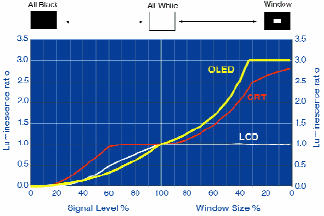
Fig. 1: A comparison of brightness vs. signal level and window size for OLEDs, LCDs , and CRTs.
Extraordinary Picture Quality
One of the great advantages of an emissive display such as an OLED display is that the dynamic range of the brightness can be controlled pixel by pixel. Figure 1 shows brightness vs. signal level and window size. The maximum brightness of a liquid-crystal display (LCD) is basically equivalent to the fixed backlight brightness, which means that it is impossible to accurately display an image that contains an extremely bright local area. This is a very important feature for TV applications because the capability of strong peak luminance would improve the impact of images dramatically – for example, a scene of fireworks at night or strong reflection of sunlight from glass could be displayed much more realistically by an OLED display.
Extremely high contrast ratio is another advantage of OLED Displays. LCDs struggle to achieve "real black," since an LCD basically works as the shutter that modulates the polarization of transmitted light from the backlight unit – this makes it extremely difficult to curtail light leakage, which in turn limits the contrast ratio. Even a tiny amount of light leakage causes considerable image degradation for some scenes in TV pictures. Imagine a forest scene during a very cloudy day; the picture level of this TV signal is very low. Under this condition, color reproduction of the deep green color of the forest on an LCD screen is degraded by a very small amount of light leakage from blue and red subpixels. However, the same scene would be much richer in color when displayed on an OLED display, in which the off-state of each subpixel is completely black – the "off" state corresponds to a non-emissive state, which means there is no light leakage. Figure 2 shows the color gamut of an OLED display and an LCD plotted vs. picture level. A wide color gamut throughout all picture levels is extremely desirable for the display of TV images. Because an OLED display is an emissive display, similar to a CRT display, its light output can be easily managed, allowing for high contrast ratios over wide viewing angles.
Moving-picture quality, another critical factor for TV performance, is evaluated by moving-picture response time (MPRT). For active-matrix displays, the MPRT is limited by the hold-type driving scheme. Recently, LCDs have overcome this problem via a high frame-rate drive (120 Hz). OLED displays can take the same approach; however, there are other ways to solve this problem. The pixel circuit of an OLED display could be designed to turn off the emission at any time in the middle of a single frame, which reduces the motion blur originated in a hold-type driving scheme, though this would result in lower overall luminance.
OLED Process for Large-Screen Displays
Sony began to sell the world's first OLED TV, the XEL-1, in December 2007 (Fig. 3). The XEL-1's 11-in. screen size is relatively small, yet it still demonstrates the outstanding picture quality promised by OLED technology, to the point where Sony believes that the potential of OLED TV is now widely recognized. So, the next question is, how large can OLED TVs be?
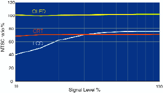
Fig. 2: The color gamut of OLED displays, LCDs, and CRT displays plotted vs. picture level.
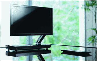
Fig. 3: Sony's XEL-1 became the first commercially available OLED TV when it hit stores in December 2007.
The XEL-1 employs vacuum evaporation of small molecules by using a metal-mask process and low-temperature polysilicon (LTPS) TFTs for the backplane. It is well recognized these technologies cannot be applied for large glass substrates; therefore, we have to develop the new technologies both for the OLED and TFT processes.
Various approaches have been proposed to achieve large-screen OLED displays. They are classified into three categories: (1) patterning by using RGB subpixels, (2) white emission plus the use of a color filter, and (3) blue emission plus color conversion. There has been vigorous debate over which type is best for large-screen-sized OLED displays.
When trying to decide which approach to take, Sony first had to determine the best way to industrialize OLED TV, for which there are really two options. The first option is to start the business with low-cost device and process technologies, followed by the improvement of performance (with the according price increases). The second is to start a business with high-performance device and process technologies (even at high costs), followed by reductions in cost. High-quality LCD and plasma TVs already permeate the market, so the next-generation TV must have superior image quality than existing flat-screen TVs. This has led Sony to the conclusion that we should choose a technology that gives us the best performance, including image quality.
A white-emission plus color-filter device has the simplest structure, so the production cost is estimated to be the lowest among these three options. Since the patterning process of the OLED layer is not required in this case, use of a metal mask is not necessary. However, power consumption is a real problem because more than two-thirds of the energy of the white emission from an OLED is absorbed by the color filter. Furthermore, this type of device gives rise to a severe tradeoff between color gamut and brightness. Adding a white subpixel (RGBW color filter) is a potentially smart way to compensate for the transmission loss caused by the RGB color filter. However, a polarizer and quarter-wavelength plate must be put on the panel to eliminate the reflection caused by the white subpixel, once again resulting in a power loss of more than 50%.
A blue-emission plus color-conversion device is better in terms of energy efficiency because basically there is no transmission lossvia the color filter, providing that color conversion efficiency is 100%. For this purpose, color-conversion materials with high conversion efficiency and low-light-scattering characteristics need to be developed.
Based on these considerations, it is concluded that an RGB-patterned-type device should be the best choice for a TV display because of its excellent image quality. For example, the XEL-1 offers a color gamut of more than 100% NTSC, a contrast ratio of 1,000,000:1,etc. So the next question is, how do we get an RGB-patterned device without using a metal-mask process in order to be able to use large motherglass, such as Gen 6 or Gen 7? An attempt to employ a solution process has been actively undertaken in a variety of methods, including polymer materials and small molecules. This seemed very attractive, and we expected this process would be realized. However, we could not achieve long lifetime with pure blue using a solution process, and this is crucial for TV application.
The concept of Sony's approach is to keep the existing device structure and vacuum-evaporation process, which has been proven to yield good enough performance and lifetimes for TV applications, and omit the metal-mask process. Figure 4 shows the cross-sectional view of the newly developed laser-transfer process that we named Laser Induced Pattern-wise Sublimation (LIPS). In this case, only the emission layer is processed by LIPS, while the other layers (hole-transport layer, electron-transport layer, etc.) are formed by using a current vapor-evaporation process. It could be thought that the metal layer on donor glass is equivalent to the heat source of the conventional vacuum-evaporation process.
TFT Backplane for Large-Screen OLED Displays
Amorphous-silicon TFT (a-Si TFT) backplanes are now widely used for active-matrix LCDs, and the manufacturing infrastructure is now well established. It is desirable to make use of a-Si TFTs as the backplane for active-matrix OLED displays. However, the threshold-voltage shifts of a-Si TFTs caused by the bias stress voltage is a serious problem for OLED displays. Compensating for the threshold-voltage shift by using driving scheme has been investigated, but it is not yet good enough to apply to TV displays; accordingly, a new TFT with a small enough threshold-voltage shift has to be developed. LTPS, which is now widely used as the backplane for OLED displays, has a very high electron mobility and extremely small threshold-voltage shift. It turns out, though, that such a high electron mobility is not really required to drive OLED displays. Microcrystalline-silicon TFTs, which have a considerably small shift in the threshold voltage and an electron mobility of 1–10 cm2/V-sec, is considered to be a good choice. The question is, what kind of process is the most appropriate to obtain microcrystalline-silicon TFTs? It is quite obvious that an as-deposited process is desirable in terms of production cost. There are many ways to conduct the as-deposited process, but none of them are available for mass production at this time. As a practical method, we developed a thermal annealing process using a high-power diode laser and named it diode Laser Thermal Anneal (dLTA). One reason we chose diode lasers is that the output laser light is very stable and controllable. When compared with eximer lasers, which are commonly used for the LTPS process, the advantage of this technology is scalability. The design of the annealing equipment is described in Fig. 5. There should not be any limit in motherglass size. We could increase the number of laser heads to improve tact time. By using this technology, we obtained an electron mobility of 2–3 cm2/V-sec and a threshold-voltage shift of ~2 V (after 100,000 hours under the bias conditions of Ids = 10 μA, 50°C), which is good enough as the backplane TFT for active-matrix OLED displays.
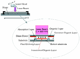
Fig. 4: A cross-sectional view of Sony's newly developed laser transfer process named Laser Induced Pattern-wise Sublimation (LIPS).
Conclusion: A New Technology Prototype
In order to realize the feasibility of this new technology as described above, Sony has developed a 27-in. OLED-display prototype (Fig. 6) with full-HD resolution (1920 x 1080 RGB). Newly developed microcrystalline-silicon TFTs and LIPS yields a picture that is just as vivid as that for the XEL-1, which makes us confident enough to employ these new technologies for manufacturing displays on larger motherglass. The significance of the 27-in. prototype is to demonstrate the possibility of large-screen OLED TVs without sacrificing picture quality. We recognize that there must be myriad different approaches in addition to ours, and we welcome the attempts that will be made to find better ways to develop high-quality low-cost OLED manufacturing technology. Those challenges will certainly improve the technological level of OLED TV and stimulate the OLED industry. •
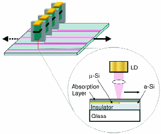
Fig. 5: A schematic of Sony's new thermal annealing process using a high-power diode laser, which it has named diode Laser Thermal Anneal (dLTA).
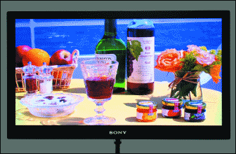
Fig. 6: Sony developed a 27-in. full-HD OLED TV prototype to test its new manufacturing technologies.
Tetsuo Urabe is a Corporate Executive SVP at Sony Corp. and the President of its Display Devices Development Group located at 4-14-1 Asahi-cho, Atsugi, Kanagawa, 243-0014 Japan; telephone +81-4-6230-6736, fax -5355, e-mail: tetsuo.urabe @jp.sony.com.