A preview of some of the most interesting papers appearing in the May 2008 issue of the Journal of the SID. To obtain access to these articles on-line, please go to www.sid.org
Edited by Aris Silzars
Motion-blur characterization on liquid-crystal displays
Wen Song
Xiaohua Li
Yuning Zhang
Yike Qi
Xiaowei Yang
Southeast University
Abstract — In this paper, several methods to characterize motion blur on liquid-crystal displays are reviewed. Based on the assumptions of smooth-pursuit eye tracking and one-frame temporal luminance integration, a simple algorithm has been proposed to calculate the normalized blurred edge width (N-BEW) and motion-picture response time (MPRT) with a one-frame-time moving-window function to LC temporal step response curves. A custom measurement system with a fast-eye-sensitivity-compensated photodiode has been developed to characterize motion blur based on LC response curves (LCRCs). MPRT values obtained by using the algorithm mentioned above and those from the smooth-pursuit-camera methods agree. Perception experiments were conducted to validate the correspondence between the simulated results and actual perceived images by the human eyes. In addition, the insufficiency of MPRT to evaluate motion blur on impulse-type light-generation LCDs, by analyzing the measurement results of a scanning backlight LCD, is discussed.
In order to make use of the LCRC, a theoretical explanation of the relationship between LCRC and motion blur needs to be developed and validated. Considering the normal three-frame LCRC, a white block represented by one horizontal line, scrolling at a speed of one pixel per frame on the screen, is given as a simple example, which is illustrated in Figs. 3(a) and 3(b), respectively. The above analysis indicates that the perceived moving picture is determined by the sum of the pixel's intensity along the motion trajectory within one frame period.
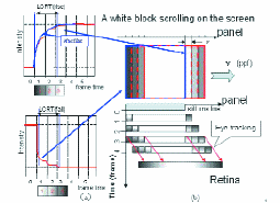
FIGURE 3 — (a) The LC response curve and (b) the illustration of a white block scrolling and eye tracking.
Transient-current asymmetry in CSTN-LCD panels
Xiaofei She
Jun Tang
Rong Chen
TPO Displays Shanghai, Ltd.
Abstract — Optical flicker is one of the artifacts of color STN-LCDs and is related to the electrical asymmetry in LCD panels. The transient-current asymmetry was observed to have a linear correlation with the internal DC offset of LC panels. The asymmetric cell structure of LC panels with a single topcoat layer leads to the asymmetry. The interface effect between different layers in an LC panel plays an important role in this phenomenon. Based on experiments, an improved RC network model was introduced to describe the mechanism.
According to previous studies, the panel asymmetry can be related to the work function of ITO electrodes, polyimide (PI) and topcoat (TC) layer structure, and the ions trapping behavior on PI layers. Therefore, the experiments were performed on three different types of test panels, which have no TC layer, a TC layer on one substrate, and a TC layer on both substrates in the cell; while the PI layers, the ITO electrodes, the process settings, and other cell configurations are the same.
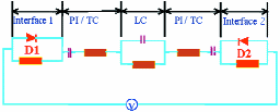
FIGURE 9 — Improved RC network model of a LC panel.
Self-bank metal conductor fabricated with silver nanoparticles
Jun Xu
Chun Fu
Yanchuan Li
Fudan University
Abstract — A novel self-bank method for fabricating a thin-film metal conductor was studied by drying silver-nanoparticle dispersion droplets. The bank of the thin-film metal conductor was created spontaneously utilizing the self-bank method. A uniform film of polymethyl methacrylate (PMMA) used as a barrier layer was formed on a glass substrate. Silver nanoparticles were dispersed in a suitable solvent for which PMMA is soluable and a silver nanoparticle fluid suspension was formed. When the silver-nanoparticle fluid suspension was injected into the PMMA film of the substrate, the solvent dissolved the PMMA film, creating a restricted area for silver-nanoparticle material defining the bank of the conductive area which improves the uniformity and conductivity of metal film. The metal conductor with a self-defined bank is formed when the PMMA film was removed after sintering. This self-bank method would be helpful in improving the deposition process of the functional materials in the fabrication of organic light-emitting diodes, organic thin-film transistors, color filters, metal electrodes, and biosensors.
One of the current problems for the ink-jet printing of thin films is related to the so-called coffee-ring effect, a ring-like film formed on the substrate. The coffee-ring effect usually refers to the non-uniform surface pattern of film due to the fluid flow of the liquid drop within the deposited area. Because the coffee-ring phenomenon strongly affects the deposited film, preventing it from achieving better physical and electrical properties, we studied a novel fabricating method of thin metal film which could improve the uniformity and electrical property of the metal conductor. This method utilizes the self-bank effect which greatly eliminates the coffee ring by forming a uniform surface.
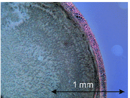
FIGURE 3 — Microphotograph of the silver thin film prepared by the self-bank effect. The bank formed on the boundary of the droplet.
Improved performance of organic light-emitting devices with ultra-thin hole-blocking layers
B. J. Chen
Y. Divayana
X. W. Sun
K. R. Sarma
Nanyang Technological University
Abstract — Tris-(8-hydroxyqunoline) aluminum (Alq3)-based organic light-emitting devices (OLEDs) using different thickness of 2,9-Dimethyl-4,7-diphenyl-1,110-phenanthorline (BCP) as a hole-blocking layer inserted both in the electron- and hole-transport layers have been fabricated. The devices have a configuration of indium tin oxide (ITO)/m-MTDATA (80 nm)/BCP (X nm)/NPB (20 nm)/Alq3(40 nm)/BCP (X nm)/Alq3 (60 nm)/Mg:Ag (200 nm), where m-MTDATA is 4, 4′,4″-Tris(N-3-methylphenyl-N-phenyl-amino) triphenylamine, which is used to improve hole injection and NPB is N,N′-Di(naphth-2-yl)-N,N′-diphenyl-benzidine. X varies between 0 and 2 nm. For a device with an optimal thickness of 1-nm BCP, the current and power efficiencies were significantly improved by 47% and 43%, respectively, compared to that of a standard device without a BCP layer. The improved efficiencies are due to a good balance between the electron and hole injection, exciton formation, and confinement within the luminescent region. Based on the optimal device mentioned above, the NPB layer thickness influences the properties of the OLEDs.
Organic multi-layered structures are necessary for lower operating voltage, higher efficiency, and practical devices. Because multi-layer-structured devices can balance hole and electron injection/transport, the light-emitting layer is far away from the metal electrode, and the mismatch of energy levels between the organic materials and the electrodes can be reduced.
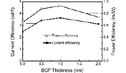
FIGURE 4 — Maximal current efficiency and power efficiency of the devices vs. the thicknesses of BCP layer.
ZnO nanowires for LED and field-emission displays
R. Könenkamp
A. Nadarajah
R. C. Word
J. Meiss
R. Engelhardt
Portland State University
Abstract — The use of ZnO nanostructures in various display applications is reported. Single-crystal-line vertically oriented nanowires with typical diameters of 100 nm and a length of 1–2 μm were grown at deposition temperatures below 100°C. Homogeneous growth over areas up to 50 cm2 on Si as well as on various metallic, transparent, and flexible substrates were obtained. Visible electroluminescence in the region between 400 and 900 nm and narrow-line near-ultraviolet (UV) electroluminescence is demonstrated. The physical conditions leading to single-crystalline growth at low temperature, the role of defects, and the possibility of doping are discussed. These issues present the main challenges on the road towards high emission rates in LED operation. Under certain conditions, sharply tipped wires can be grown that hold promise for field-emission applications.
ZnO has long been considered a strong candidate for lighting and display applications. Its bandgap of 3.37 eV allows for the generation of photons over the entire visible spectral range, and the large exciton binding energy of 60 meV promises high excitonic transition probabilities. Various defect transitions involving impurities as well as vacancies are known to produce light emission at distinct colors in the visible. Generation of white and colored light therefore appears feasible. ZnO nanowires can be fabricated by a variety of methods, including CVD, MOCVD, PVD, solution growth, and electrodeposition. Our own work has focused on electrodeposition from aqueous solutions because this method produces single-crystalline wires at comparatively low temperatures on practically any conductive substrate.
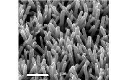
FIGURE 1 — Single-crystalline ZnO nanowires deposited on SnO2-coated glass at 85°C in electrodeposition.
Design of carbon nanotubes for large-area electron field-emission cathodes
Richard C. Smith
S. R. P. Silva
University of Surrey
Abstract — Electron-field-emission displays offer a viable option for the next generation of flat-panel screens. Boasting high-quality images in terms of good color saturation, fast refresh rate, and high brightness, these displays have the potential to offer above and beyond what the current market leaders, LCD and plasma. However, for the realization of such a new display disrupting the incumbent LCD and plasma displays, not only does the image quality need to be better, but fabrication costs and suitable manufacturing processes need to be in place at reduced cost. Many viable cathode materials have been proposed in recent years, one of which being the use of carbon nanotubes (CNTs) in various forms (aligned growth, screen printing, and polymer matrix). In this review, a series of recent experiments investigating the field-emission characteristics of carbon-nanotube systems for possible use in the display industry is presented.
Following an introduction into the phenomenon of field emission, some computational simulations investigating the geometric field-enhancement factor were examined. This effect is first discussed in terms of a single, isolated CNT, then secondly for an array of CNTs. To expand on these findings, the use of nano-manipulators in order to accurately determine the FE characteristics of CNT experimentally is reported. The third and fourth sections of this review involve reporting on incorporating CNTs within a polymer matrix, and also that of room-temperature-grown CNTs for large-area applications.
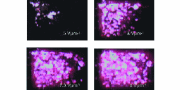
FIGURE 9 — Emission-site density maps made over a 3-mm2 area from a 20% B-doped MWNT-PS composite at different applied fields. The maps are taken over the same area with applied fields of 5, 6, 7, and 8 V/μm.
Characteristics of an electron source of a surface-conduction electron-emitter display
Chuanxing Wu
Weijun Xu
Xin Lei
Chunliang Liu
Shengli Wu
Wenbo Hu
Zhihu Liang
Xi'an Jiaotong University
Abstract — The electron source is an essential part of a surface-conduction electron-emitter display (SED). An electron source for an SED was obtained after certain procedures were performed. By introducing a carbon atmosphere, the electron-emission characteristics of an SED were studied experimentally. The electron-emission characteristic curves were drawn after comparing the experimental data of the electron source obtained in a vacuum environment with the data obtained in a carbon atmosphere, from which it had proved that a carbon atmosphere could significantly improve the electron-emission characteristics of an SED. As a result, both the device current and the emission current had become stronger and the efficiency of surface-conduction electron emission had been improved significantly. The possible reasons were analyzed: more carbon, which could possibly form the electron-emission region of an SED, was produced from the carbon atmosphere during the electrical activation process.
When forming the conductive film, three types of Pd organic solutions were adopted with a Pd concentration of 0.25, 0.5, and 1%, respectively. Here, a triangular wave was applied as the device voltage Uf with a peak value of 30 V. Meanwhile, no anode voltage was applied. However, the activation time needed for the three kinds of conductive film were different. It took a relatively long time – about 2 hours – for the formation of condutive film and activation of the 0.25%-Pd film as a result of its relatively high resistance. When dealing with the 0.5%-Pd film, it took only less than 1 minute before the device current If dropped dramatically from 1 A to 0.008 mA with its resistance increasing from 266 Ω to 10.2 kΩ. The device current If ranged from 0 to 11 mA, and the emission current Ie ranged from 0 to 4.5 μA.
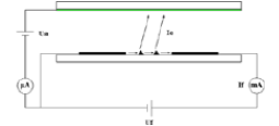
FIGURE 4 — The circuit.
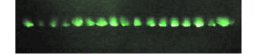
FIGURE 5 — A photograph of SED luminous spots (Ua = 750 V).
Dynamic studies on the charging of spacers for high-voltage field-emission displays
Hao Li
Dirk C. Jordan
Bernard F. Coll
Emmett Howard
Scott V. Johnson
Michael R. Johnson
Kenneth A. Dean
James E. Jaskie
Motorola, Inc.
Abstract — In this article, a systematic study on the relationship between the rate of spacer surface-charge accumulation and the anode voltages in a dynamic setting is presented. The spacers are placed in a test package simulating a field-emission panel where electron trajectories are recorded along a preset timeline. True secondary emission of spacers under the influence of an anode field is then deduced and the factors affecting the rate of charge accumulation on the spacer surface are discussed. The results of invisible spacers under different operating conditions of anode voltage, emission current, and pulse width will also be given.
Figure 3 shows actual anode images at different stages of the charging process in the spacer test fixture. The vertical lines are rows formed by individual subpixels. A spacer was placed in between the two rows in the center. The anode voltage was set at 10 kV. The primary beam was pulsed with a pulse width of 15 μsec and the emission current was set at 1.5 μA per subpixel.
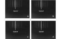
FIGURE 3 — Spacer-charging process in FED operating at 10 kV. Primary electron dosage per subpixel are: (a) 22.5, (b) 157.5, (c) 180, and (d) 202.5 pC, respectively.
Film surface morphology and field-emission characteristics of a carbon-nanotube array pattern fabricated under a magnetic field
I.-S. Tsai
C.-W. Huang
H.-K. Huang
J.-M. Jehng
T.-C. Pan
Feng Chia University
Abstract — This study focuses on the influence of sodium metasilicate binder on CNT paste and the arrangement of Mg–Ni alloy multi-walled carbon nanotubes on the surface of CNT film under the influence of a magnetic field. The CNT paste was prepared by mixing CNTs with silver epoxy resin and sodium metasilicate solution and coating them onto the surface of indium tin oxide (ITO) glass. The impact of sodium metasilicate solution and magnetic strength on the morphology of the paste film's surface and on the field-emission (FE) characteristics of the cathode was examined. The experimental results showed that the CNT paste provided good adhesion between the CNT array and silver epoxy resin when sodium metasilicate solution was presented. CNT paste containing sodium metasilicate showed a better dispersion with silver epoxy resin and a better CNT-array pattern, and better vertical alignment of the CNT was obtained when the magnetic field and grid were both applied. An optimal condition for a better CNT-array pattern for both the morphology and FE characteristics had a magnetic strength of 189 mT, magnetization time of 30 min, and a grid above the cathode.
In this study, we tried to solve the problem of covering CNTs with CNT paste by using two approaches. One approach was to add an inorganic binder as filler and to dilute the viscosity of the CNT paste so as to let the CNTs protrude out of the film's surface without being covered by silver epoxy resin. Another approach was to use a magnetic force to pull on one end of each magnetized CNT while the other end of the CNT was fixed by the paste. Under a magnetic field, one end of the CNT will be pulled by the magnetic force and bent upward toward a position parallel to the magnetic field (and perpendicular to the ITO glass) as shown in Fig. 3.
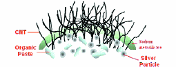
FIGURE 3 — Schematic diagram shows that the one end of the CNT is pulled by a magnetic force and bent upward.
Growth of uniform carbon-nanotube arrays with sandwich technology
Zexiang Chen
Qiang Zhang
Bingjin Zhu
Daniel den Engelsen
Peter K. Bachmann
Astrid Lewalter
University of Electronic Science and Technology of China
Abstract — In this work, a novel approach to grow structured, highly oriented carbon nanotubes (CNTs), which are vertically aligned to the substrate and show large field emission, is reported. Growth is performed on lithographically defined dots of catalysts, which can be deposited on metallic, semi-conducting, and glass substrates. A sandwiched catalyst structure and microwave plasma chemical vapor deposition enables the formation of uniform CNT arrays of 1.6 x 1.6 μm2. The method is easily scalable to large areas. The CNT arrays exhibit a stable field emission of 20 mA and a macroscopic current density of 50 mA/cm2 at a rather low electric field of 5.33 V/μm. Modeling of space charge indicates that space charge reduces the magnitude of the CNT emission at high field strength: this agrees satisfactorily with the measurements.
Figure 1(a) illustrates a standard lithographic method to pattern a Fe-catalyst layer for CNT growth on a silicon wafer. Figure 1(b) shows the final structure of the CNT bundles or arrays having a diameter of 1.6 μm and separated from each other at a pitch of 15 μm. First, a layer of titanium nitride (TiN) was sputtered on a silicon substrate covered with a photoresist pattern, then a thin layer of aluminum was deposited on top of the TiN layer by evaporation, and finally a layer of iron was evaporated to act as a source for the catalyst particles. By stripping the photoresist layer, the structure as shown in Fig. 1(a) was obtained.
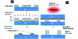
FIGURE 1 — (a) Sketch of fabrication of catalyst arrays. (b) Sketch of sandwich growth of CNTs.
Suspension-deposited carbon-nanotube networks for flexible active-matrix displays
Axel Schindler
Stefan Spiessberger
Steffen Hergert
Norbert Fruehauf
James P. Novak
Zvi Yaniv
University of Stuttgart
Abstract — The unique properties of carbon nanotubes (CNTs) promise innovative solutions for a variety of display applications. The CNTs can be deposited from suspension. These simple and low-cost techniques will replace time-consuming and costly vacuum processes and can be applied to large-area glass and flexible substrates. Single-walled carbon nanotubes (SWNTs) have been used as conducting and transparent layers, replacing the brittle ITO, and as the semiconducting layer in thin-film transistors (TFTs). There is no need for alignment because a CNT network is used instead of single CNTs. Both processes can be applied to glass and to flexible plastic substrates. The transparent and conductive nanotube layers can be produced with a sheet resistance of 400 Ω/4 at 80% transmittance. Such layers have been used to produce directly addressed liquid-crystal displays and organic light-emitting diodes (OLEDs). The CNT-TFTs reach on/off ratios of more than 105 and effective charge-carrier mobilities of 1 cm2/V-sec and above.
FIGURE 3 — Fully processed CNT-network TFTs on a 50 x 50 mm2 PES substrate.
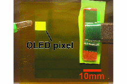
FIGURE 6 — A 5 x 6-mm2 OLED with a CNT-network anode at 5-V driving voltage under illumination of a fluorescent tube.