Transparent Conductive Oxides for Display Applications
The search for a cost-effective replacement for indium tin oxide (ITO) for flat-panel displays continues. This article describes a practical solution of high-accuracy patterning of fluorine-doped tin oxide (FTO), making FTO an attractive replacement for ITO for PDPs.
by Harm Tolner, Bernard Feldman, Douglas McLean, and Chris Cording
TRANSPARENT CONDUCTING OXIDES (TCOs) are widely used in solar cells, as front electrodes in flat-panel displays (FPDs), electromagnetic shielding windows, touch-sensitive control panels, low-emissivity windows in refrigerators, cold heat mirrors, etc.(Fig. 1). Tin-doped indium oxide (ITO) is the standard transparent conductor (TC) used for practically all flat-panel displays (FPDs) manufactured today. However, indium is a relatively rare and expensive element to extract from the earth; consequently, there is mounting pressure to find a less costly replacement.
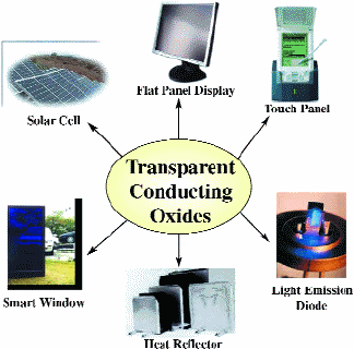
Fig. 1: Applications of TCOs.1
The market for ITO has recently been analyzed by Displaybank, as shown in Fig. 2. Replacement criteria for ITO differ for the two most common FPD technologies: liquid-crystal displays (LCDs) and plasma-display panels (PDPs). Because the TC of the active TFT plate is deposited after the deposition of the transistors for LCDs, high-temperature conditions are not permissible. Therefore, sputtering of the TC is the primary means of deposition. Several approaches to replace ITO for the active plate of LCDs are described by Miniam2 and Osono et.al.,3 but thus far, noindustrially acceptable solution has been found.
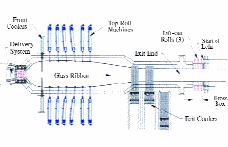
For PDPs, on the other hand, the TC is deposited directly on a glass surface before the other processing steps. Therefore, a high-temperature process can be used as long as it does not exceed the annealing temperature of the substrate glass. Chemical vapor deposition (CVD) at high temperature (~600°C) can allow the deposition of the TC on glass as the glass is made (see Fig. 3).
Typically, the cost of an ITO layer, deposited by sputtering, constitutes more than 80% of the TCO-layer cost in a PDP and is of the same order of magnitude as the cost of the PDP glass plates. This will likely increase within a few years because there will be a shortage of indium, endangering the stable supply of ITO. This is not a positive prospect for FPD makers, who have seen market forces drive down flat-panel-TV prices by about 30% per year. The manufacturers need to realize cost savings to match these price reductions, and a likely candidate is to reduce the cost of the TCO material and the cost of the TCO deposition process.
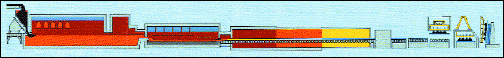
For PDPs, the replacement of ITO by tin oxide (SnO2) is an obvious candidate. Thanks to the new proprietary wet-chemical process described in this article, tin oxide now can be patterned accurately in the form of discharge electrodes. Fluorine-doped tin oxide (FTO) has an especially low resistance, comparable to that of ITO, and can be deposited on the glass production float-line using a CVD process (Fig. 4). By using deposition onto the glass after solidification at 600°C, the cost of annealing, needed to achieve a low resistance, is also reduced. This process is described in detail by Dong-Ki Min and Sae-Young Kim1 and T. Ishida et al.4 and has been demonstrated with good success. Tin oxide has been overlooked because it could not be patterned easily by photolithography, unlike ITO.
This article describes a practical solution of high-accuracy patterning of FTO, making FTO an attractive replacement for ITO for PDPs as well as other applications using a transparent conductor on a glass surface, such as touch screens and solar panels.
Fundamentals of TCOs
While conductivity and transparency are usually mutually exclusive properties, this apparently is not the case for TCOs. So what is the secret behind this unique property of TCOs?
The high visual transparency of TCOs is the result of the high value of the electronic bandgap Eg (see Fig. 5). For TCO, it is higher than 3.0 eV, corresponding to the energy of a 400-nm blue photon. So, visible photons (having an energybetween 2 and 3 eV) cannot excite electrons from the valence band (VB) to the conduction band (CB), and hence are transmitted through it.
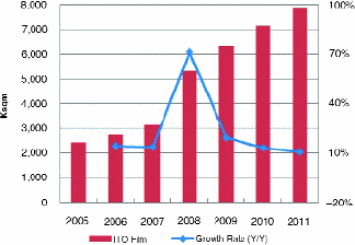
Fig. 2: Global ITO film production capacity. (Source: Displaybank, In-depth Analysis: Touch-Screen Panel Industry Trends and Business Strategies.)
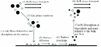
Fig. 3: Schematic representation of the basic steps in a chemical vapor deposition process.5
On the other hand, electrons from the donor level to the CB (for an n-type TCO) or holes from the acceptor level to VB (for p-type TCO), generate appreciable conductivity.
In the case of fluorine-doped tin oxide (FTO), the fluorine is responsible for the creation of a donor level. For tin oxide (SnO2) the bandgap is 3.6–4.0 eV.
UV light, with an energy higher than the bandgap energy Eg, is fully absorbed by the TCO, while visible light is transmitted. The donor level demonstrates high conductivity.
For most applications, n-type TCOs are used because they exhibit the highest conductivity at a transparency of 80% or more. In a semi-conductor, the hole mobility is much lower than the electron mobility, explaining the much higher conductivity of n-type TCOs, such as FTO and antimony-doped tin oxide (ATO).
FTO Characteristics
• FTO is deposited on the float glass line as the glass is made; a low-cost process compared to that for sputtered ITO.
• High-temperature deposition on the float- line (~600°C) eliminates any organic contamination so that post-deposition firing of the coated glass is not required by PDPs.
• High-temperature CVD guarantees superior film adhesion by virtue of the chemical modification of the surface.
• The hardness of FTO on the Mohs scale is 6.5; glass is 6 and ITO is ~5. If FTO film is scratched with a razor blade, steel will be wiped onto the FTO film. A harder-than-glass film permits direct electrical contact and eliminates film scratches during processing, thus enhancing product yield.
• The resistivity of FTO barely changes when fired on a PDP front plate at 570–580°C, contrary to the case for ITO. For example, whereas the resistivity of 30-Ω/sq. ITO film increases up to 90–100 Ω/sq. after firing, together with the transparent dielectric layer of a PDP at 580°C, the corresponding change for FTO is < 10%. Thus, a 100-Ω/sq. FTO film can replace a 30-Ω/sq. ITO film with similar resistance after the application of the dielectric overglaze for PDPs.
• The net visual transmittance for glass and film is 86% for FTO vs. 84% for the thicker ITO coating.
• Because the etching is performed at room temperature with much lower HCl concentrations than used in current ITO etching, there is no mist problem.
Patterning of FTO by Wet Chemical Etching
Typically, the gap control in a PDP has to be accurate within 3% (3-sigma) of the TCO gap size, so an edge definition of ±1 μm is required. Figure 6 shows the result of the new etching process applied on FTO. The etching time is less than 1 minute at room temperature and the process uses benign and dilute low-cost chemicals and is readily automated.
In Fig. 6, the 6- and 12-μm etched lines andspaces (bottom) are compared with the original photoresist pattern (top). If the resist edge and the etched structure are superimposed, there is better than 0.1-μm agreement. This is a conse-quence of the special penetration control in our etch process explained below in some detail.
 (a)
(a)
 (b)
(b) 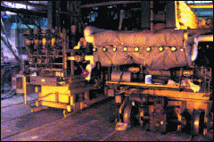 (c)
(c)
Fig. 4: (a) Glass float-line overview; (b) detailed view of the front part; and (c) CVD reactor on the float-line. http://www.icmm.csic.es/ ingesnet/presentaciones2006/Surface%20Treat%20Glass%20(J%20Marco).pdf.
The undercut is only ~0.9 μm for a 1.5-μm-thick S1818 photoresist (Rohm & Haas). When a thick dry film resist (DFR) is used (e.g., TOK), then the undercut is about 3.0 μm.
Characteristics of the New Tin Oxide Etching Process9
The etching of FTO introduces a new complication not present when using ITO. Most metal oxides, including ITO, can be reduced to the metal by using hydrogen ions in strong acid solutions. FTO cannot be reduced in this way.
However, if zinc particles are added to the acid, then FTO can be etched because of electron transfer from the zinc to FTO. In this well-known process, the FTO surface is negatively charged by the electrons from the zinc; it then attracts H3O+ ions and reduces them to H atoms, which diffuse into the lattice and reduce Sn4+ to metallic tin, breaking up (etching) the FTO.
This electrochemical process can also be described as the action of multiple short-circuited 1.34-V batteries, each with negative Zn and positive FTO poles in acid electrolyte. The overlapping etch zones of the multiple batteries guarantee a complete etch of uncovered FTO.
In this normal FTO etching process just outlined, the H atoms that diffuse under the resist areas, however, can cause a drastic and uneven undercut, resulting in an edge definition that is completely unacceptable by the display industry.
In our new process,6 this atomic-hydrogen diffusion is controlled by adding metal ions (Fe2+, for example) to the electrolyte so that metal is deposited on the FTO along with the production of H atoms. Buildup of the deposited metal continues the battery action but slows the diffusion of H atoms into the lattice (penetration control), thereby controlling undercut.
The battery action proceeds at the same time as the direct action of Zn with hydrogen ions to produce diatomic hydrogen gas, although this reaction has no etching effect. Zn overvoltage slows the direct reaction to the point where it does not out-compete the battery action.
When the FTO lattice has completely broken up, the remaining metal (Sn) and reduced penetration control metal (which does not dissolve in the electrolyte) is removed in a subsequent operation (using acidified Fe,3+ for example) to complete the etch.
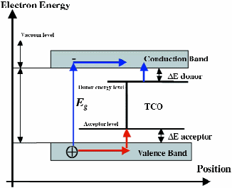
Fig. 5: Energy levels involved in a TCO. For fluorine-doped tin oxide (FTO), the fluorine is responsible for the creation of a donor level. For tin oxide (SnO2), the bandgap is 3.6–4.0 eV.
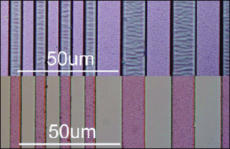
Fig. 6: FTO pattern (bottom) after wet chemical etching of 6- and 12-μm-wide lines and spaces, compared with the resist pattern (top). The resist used is a 1.5-μm-thick S1818 photo-resist from Rohm & Haas.
In the new process, the only change is the use of a zinc acid slurry instead of the usual acid etch. The etching time is not increased. For an example of the automation of the etching machine, go to www.feldmantechnology.com.7
Although we have cited advantages of FTO vs. ITO, it is important to note that we have demonstrated the same properties for the etch-ing of ITO by our new process with penetration control as an alternative to the harsh liquid-chemical etch currently employed commercially.
FTO Use in High-Definition and High-Efficiency Plasma Displays
In a plasma display, VUV light is generated in a neon–xenon plasma by triggering a discharge across a narrow gap of about 80 μm in the TCO electrodes (see Fig. 7).
The phosphor on the opposite plate converts the 147- and 173-nm radiation into visible light, and this in turn is transmitted toward the viewer through the transparent electrodes.
In order to reduce the PDP power consumption, the efficiency must be increased. This is possible by using a much higher xenon pressure than the standard 10% xenon. Unfortunately, this also increases the firing voltage, partially reducing the gain in efficiency. The solution is to reduce the TCO gap. As shown by Oversluizen et al.,9 40% or more xenon can then be used and an efficacy of 5 lm/W can be achieved.
Until recently, this operational mode could not be used because of the increase in addressing jitter. However, the invention of new types of MgO coating, such as the crystal emissive MgO layer (CEL) developed by Pioneer, has changed all of this. The new etching process will enable us to use 60 μm or even smaller gaps, with an accuracy better than 3%, enabling high manufacturing yields.
Therefore, the new etching technology opens the door widely for PDP power reduction in true high-definition 1080-line PDPs for both FTO and standard ITO.
Conclusion
This article describes a practical solution for high-accuracy patterning of metal oxides, especially fluorine-doped tin oxide (FTO), which cannot be patterned accurately by any other means. Thus, FTO is a suitable replacement for ITO, especially for PDPs. The etching method can be applied to FTO coatings applied off the glass float line, but the big cost savings occur when the FTO is applied in-line as the glass is made.
At the present time, to the best of our knowledge, FTO is available in-line only on soda-lime glass over an SiO2 barrier. This application has been shown to work for PDPs that use striped electrodes as shown in Fig. 7.
However, to be able to compete with LCDs, a 2-D-electrode pattern more complicated than stripes (e.g., T-shaped electrodes) is required to obtain high-definition PDP performance. Unfortunately, the glass is distorted and the required accuracy of the 2-D electrode pattern is lost when the dielectric overglaze is fired at ~570°C.
What is required for full utilization of our process for PDPs is either the development of a lead-free overglaze that fires clear at <520°C or the deposition of FTO on the high-strain- point glass currently in use for PDP fabrication. Hopefully, this article will inspire one of these developments
References
1D-K. Min and S-Y. Kim, "Transparent Conducting Oxides," Yonsei University, 6.4 (2002).
2T. Minami, "Transparent conducting oxide semiconductors for transparent electrodes," Semiconductor Science and Technology 20, S35-S44 (2005).
3Isono et al., "Highly conductive SnO2 thin films for flat-panel displays," J. Soc. Info. Display 15/2, 161 (2007).
4T. Ishida et al., "Highly conductive transparent F-doped tin oxide films prepared by photo-CVD and thermal-CVD," Thin Solid Films281/282, 228–231 (1996).
5A. M. B van Mol, Ph.D. thesis, "Chemical Vapor Deposition of Tin Oxide Thin Films," Technical University of Eindhoven, The Netherlands (ISBN 90-386-2715-7); available for free on the Internet at: http://alexandria. tue.nl/extra2/200313223.pdf.
6U.S. Patents 5,976,396; 6,174,452; 6,180,021; 6,193,901; 6,180,021; 6,749,766; 7,115,212.
7See movie at www.feldmantechnology.com.
8J. P. Boeuf, "Topical Review: Plasma display panels: physics, recent developments, and key issues," J. Phys. D: Appl. Phys. 36, R53–R79 (2003).
9G. Oversluizen, et al., "Plasma display panel design for simultaneous high efficacy and high luminance," J. Appl. Phys.103 (1), 13301 (2008).•
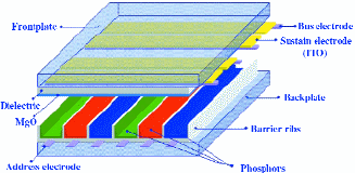
Fig. 7: The PDP cell design.8 The front plate and back plate are shown separated in this picture (exploded view). The narrow gap (~ 80 μm) between the transparent scan and sustain electrodes determines the discharge voltage.
Harm Tolner is a Display Consultant with Tolner Technology, De Genestetlaan 11, Eindhoven, 5615 EG, The Netherlands; telephone +31-62-0614731, e-mail: h.tolner1@ chello.nl. Douglas McLean is a Chemistry Consultant located in Los Gatos, California; e-mail: jmclean@jps.net. Bernard Feldman is President of Feldman Technology, Watsonville, California; e-mail: ftc@cruzio. com. Chris Cording is Corporate Development Manager for AGC Flat Glass North America, Inc., Church Hill, Tennessee; e-mail: Chris.Cording@na.agc-flatglass.com.