A preview of the papers appearing in the November 2007issue of theJournal of the SID. To obtain access to these articles on-line, please go to www.sid.org
Edited by Aris Silzars
Human factors of 3-D displays
Robert Patterson
Washington State University
Abstract — This paper provides a selected review of a number of important perceptual and human-factors issues that arise when 3-D displays are designed and used. This review and analysis draws heavily from the basic vision literature in order to help provide insight for future design solutions for 3-D displays. Issues discussed include (1) the basics of human stereopsis, (2) interocular crosstalk, (3) oculomotor responding and distance scaling of binocular disparity information, (4) accommodative-vergence mismatch, and (5) stereoanomly. The paper concludes with a presentation of several recommendations for the design of 3-D displays.
The technology behind stereoscopic displays is more developed, and more widely used, than those based on holography or volumetric methods. Thus, many of the human factors and perceptual issues that arise with 3-D displays have been articulated within the context of stereoscopic displays, with very few formal studies being conducted on the visual perception of holographic or volumetric displays. Despite this diversity in delivery systems, in the final analysis it is the binocular visual system to which the binocular parallax information is being presented. This means that, from a human-factors perspective, there are common issues and problems that need to be addressed and solved when any type of 3-D display is designed.
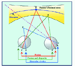
FIGURE 1 — Drawing depicting the basics of stereoscopic viewing.
Efficiency analysis for multi-view spatially multiplexed autostereoscopic 2-D/3-D displays
Graham J. Woodgate
Jonathan Harrold
Ocuity, Ltd.
Abstract — The wide-viewing freedom often requested by users of autostereoscopic displays can be delivered by spatial multiplexing of multiple views in which a sequence of images is directed into respective directions by a suitable autostereoscopic optical system. This gives rise to two important design considerations – the optical efficiency and the resolution efficiency of the device. Optical efficiency is particularly important in portable devices such as cell phones. A comparison is given between lens and barrier systems for various spatial multiplexing arrangements. Parallax-barrier displays suffer from reduced optical efficiency as the number of views presented increases whereas throughput efficiency is independent of the number of views for lens displays. An autostereoscopic optical system is presented for the emerging class of highly efficient polarizer-free displays. Resolution efficiency can be evaluated by investigating quantitative and subjective comparisons of resolution losses and pixel appearance in each 3-D image. Specifically, 2.2-in.-diagonal 2-D/3-D panel performance has been assessed using Nyquist boundaries, human-visual contrast-sensitivity models, and autostereoscopic-display optical output simulations. Four-view vertical Polarization-Activated Microlens technology with either QVGA mosaic or VGA striped pixel arrangements is a strong candidate for an optimum compromise between display brightness, viewing angle, and 3-D pixel appearance.
Typically, autostereoscopic displays use elongated optical structures (such as cylindrical lenses), cooperating with columnar pixel structures in which a white pixel comprises three color subpixels arranged in stripe or mosaic configurations. Delta pattern pixels are commonly used in 2-D displays, but usually result in overlapping pixel data within a single column in 3-D, thereby increasing crosstalk. The appearance of the 3-D image for a single eye compared to the arrangement of the same base 2-D panel and associated autostereoscopic optical element is described.
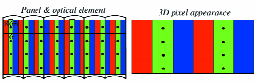
FIGURE 5
Moiré interference in multilayered displays
Gareth Bell
Robert Craig
Tony Simmiss
PureDepth, Inc.
Abstract — Multi-layered displays contain a pair of parallel liquid-crystal-display panels spaced apart from each other. The viewer sees objects displayed on the front and rear layers to form a three-dimensional image. Each layer has an array of pixels arranged in an RGB striped configuration. When imaged on the retina, the layers interact to produce a beat pattern referred to as moiré. This pattern can be distracting to people seeking to use a multi-layered display. To solve this problem, the high-frequency components on the rear most display are attenuated using an interstitial optical diffuser. Given the characteristics of the diffuser and imaging planes, a function is derived to calculate the amount of residual moiré interference present. A measurement device and methodology was constructed to quantify the amplitude of the beat pattern and the blur on the rear image plane in terms of the human visual system.
A diffuser is placed between the liquid-crystal-panel layers to attenuate the moiré interference [shown in Figs. 1(b) and 1(c)] generated by the regular arrays of pixels. Both the properties of the diffuser and its distance from the display layer affect the amount of blur and the corresponding amplitude of moiré interference on the rear image. Given the periodic nature of components involved, and the spatial-frequency channel description of the human visual system, conversion of the problem into the Fourier domain has provided a single equation predicting the amount of visible residual moiré and blur.
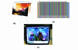
FIGURE 1 — The moiré interference problem in multi-layered displays (MLDs). (a) An MLD system consists of stacked LCD panels to produce a layered image. The color filters (b) and black matrix in the stacked panels interact with each other to form moiré interference (c).
Characterizing crosstalk in anaglyphic stereoscopic images on LCD monitors and plasma displays
Andrew J. Woods
Ka Lun Yuen
Kai S. Karvinen
Curtin University of Technology
Abstract — In 1853, William Rollman developed the inexpensive and easy to use anaglyph method for displaying stereoscopic images. Although it can be used with nearly any type of full-color display, the anaglyph method compromises the accuracy of color reproduction, and it often suffers from crosstalk (or ghosting) between the left- and right-eye image channels. Crosstalk degrades the ability of the observer to fuse the stereoscopic image, and hence reduces the quality of the 3-D image. Crosstalk is present in various levels with most stereoscopic displays; however, it is often particularly evident with anaglyphic 3-D images. This paper summarizes the results of two projects that characterized the presence of anaglyphic crosstalk due to spectral issues on 13 LCD monitors, 14 plasma displays, and a CRT monitor when used with 25 different pairs of anaglyph 3-D glasses. A mathematical model was used to predict the amount of crosstalk in anaglyphic 3-D images when different combinations of displays and glasses are used, and therefore highlight displays, glasses, and combinations thereof which exhibit lower levels of crosstalk when displaying anaglyphic 3-D images.
Figure 1 provides an illustration of the process of crosstalk in anaglyph stereoscopic images due to spectral leakage (as illustrated for the red/cyan method). Firstly, the display has a specific spectral output for the red, green, and blue color channels. Usually the left perspective image is stored in the red color channel and the right perspective image is stored in the green and blue color channels (cyan). Second, the red/cyan anaglyph 3-D glasses used to view the anaglyph display also have a certain spectral transmission response for the left and right eye filters.
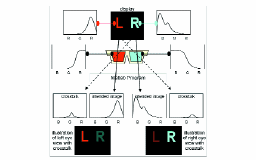
FIGURE 1 — Illustration of the process of anaglyph spectral ghosting and its simulation in this project.
Development of a 42-in. 2-D/3-D switchable display using multi-view technology for public-information-display applications
K. J. Kim, H. Kang,
M. K. Jang, B. C. Ahn,
I. J. Chung, T. S. Park,
J. W. Chang, K. I. Lee,
S. T. Kim
LG.Philips LCD
Abstract — A 42-in. 2-D/3-D switchable display operating in a parallax-barrier-type system consisting of liquid-crystal displays (LCDs) has been developed. The system displays 2-D images in full resolution, without any degradation to the original 2-D images, and 3-D autostereoscopic images with resolutions higher than SVGA with wide viewing zones electrically controlled by the parallax-barrier system. The system is intended for use in public-information displays (PIDs), a booming field, and as displays for gaming, medical, and simulation applications.
Figure 2 shows the functions of a 2-D/3-D switchable display which is combined with the main LCD and the switchable LCD. In 2-D mode, the main LCD displays conventional 2-D images from the PC. The switchable LCD is turned off; this means that the display does not generate a binocular parallax because barrier patterns are not created. The control unit decreases the luminance of the BLU for the convenience of viewers because it generates a very high luminance in the 2-D mode as compared with the 3-D mode. In 3-D mode, the main LCD displays interweaved 3-D images from the PC. When the switchable LCD is turned on, it generates a binocular parallax by displaying barrier patterns.
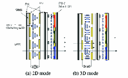
FIGURE 2 — Cross-sectional views of a parallax-barrier shutter. (a) 2-D mode without supplying electrical power to the switchable LCD (b) 3-D mode with power applied to the switchable LCD.
A systematic framework for on-line calibration of a head-mounted projection display for augmented-reality systems
Hong Hua
Chunyu Gao
University of Arizona
Abstract — Augmented reality (AR) is a technology in which computer-generated virtual images are dynamically superimposed upon a real-world scene to enhance a user's perceptions of the physical environment. A successful AR system requires that the overlaid digital information be aligned with the user's real-world senses – a process known as registration. An accurate registration process requires the knowledge of both the intrinsic and extrinsic parameters of the viewing device and these parameters form the viewing and projection transformations for creating the simulations of virtual images. In our previous work, an easy off-line calibration method in which an image-based automatic matching method was used to establish the world-to-image correspondences was presented, and it is able to achieve subpixel accuracy. However, this off-line method yields accurate registration only when a user's eye placements relative to the display device coincides with locations established during the offline calibration process. A likely deviation of eye placements, for instance, due to helmet slippage or user-dependent factors such as interpupillary distance, will lead to misregistration. In this paper, a systematic on-line calibration framework to refine the off-line calibration results and to account for user-dependent factors is presented. Specifically, based on an equivalent viewing projection model, a six-parameter on-line calibration method to refine the user-dependent parameters in the viewing transformations is presented. Calibration procedures and results as well as evaluation experiments are described in detail. The evaluation experiments demonstrate the improvement of the registration accuracy.
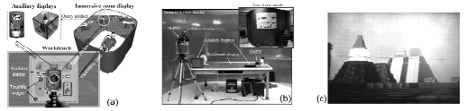
FIGURE 2 — SCAPE: a multi-scale collaborative augmented virtual environment: (a) conceptual simulation of SCAPE; (b) a prototype implementation; (c) a sample view through the surrounding wall display.
Circuits using uniform TFTs based on amorphous In–Ga–Zn–O
Ryo Hayashi, Masato Ofuji,
Nobuyuki Kaji, Kenji Takahashi,
Katsumi Abe, Hisato Yabuta,
Masafumi Sano, Hideya Kumomi,
Kenji Nomura, Toshio Kamiya,
Masahiro Hirano, Hideo Hosono
Canon Research Center
Abstract — High-performance and excellent-uniformity thin-film transistors (TFTs) having bottom-gate structures are fabricated using an amorphous indium–gallium–zinc-oxide (IGZO) film and an amorphous-silicon dioxide film as the channel layer and the gate insulator layer, respectively. All of the 94 TFTs fabricated with an area of 1 cm2 show almost identical transfer characteristics: the average saturation mobility is 14.6 cm2/(V-sec) with a small standard deviation of 0.11 cm2/(V-sec). A five-stage ring-oscillator composed of these TFTs operates at 410 kHz at an input voltage of 18 V. Pixel-driving circuits based on these TFTs are also fabricated with organic light-emitting diodes (OLEDs) which are monolithically integrated on the same substrate. It is demonstrated that light emission from the OLED cells can be switched and modulated by a 120-Hz ac signal input. Amorphous-IGZO-based TFTs are prominent candidates for building blocks of large-area OLED-display electronics.
Besides the high performance and low-temperature processability, the transparent amorphous-oxide semiconductors (TAOS) TFTs are expected to exhibit good short-range uniformity in their characteristics as those of a-Si:H TFTs because of the amorphous nature of the active-layer material. The short-range uniformity is important in almost all of the applications of TFTs. For example, active-matrix flat-panel displays (AMFPDs) require good uniformity of the backplane TFTs for smooth rendering of the displayed images. Particularly, active-matrix organic light-emitting-diode (AMOLED) displays demand uniformity at the highest level because every pixel is driven by a circuit composed of two or more TFTs.
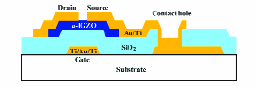
FIGURE 5 — Cross-sectional schematic of the a-IGZO channel bottom-gate top-contact TFT constituting the ring oscillator.
Active-matrix OLED backplanes based on LTPS for small molecules and polymers
Efstathios Persidis
Holger Baur
Steffen Hergert
René Hlawatsch
Fabio Pieralisi
Patrick Schalberger
Norbert Fruehauf
University of Stuttgart
Abstract — A four-mask low-temperature poly-Si (LTPS) TFT process for p- and n-channel devices has been developed. PECVD-deposited amorphous silicon was recrystallized to polycrystalline-silicon with single-area excimer-laser crystallization, while the gate dielectric was fabricated by PECVD deposition of a SiH4–N2O-based silicon oxide. Formation of drain and source was carried out with self-aligned ion-beam implantation. To prove the potential capa-bility of these devices, which are suitable for conventional and inverted OLEDs alike, several functional active-matrix backplanes implementing different pixel circuits have been produced. This active-matrix backplane process has been customized to drive small molecules as well as polymers regardless if its structure is top or bottom emitting.
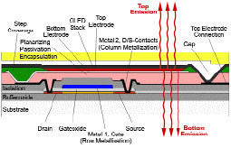
FIGURE 2 – Cross-sectional view of an AMOLED display.
FIGURE 10 — Photograph of a fabricated 1-in. AMPLED display.
Novel mobile TFT-LCDs based on SLS technology
Jae Beom Choi
KeeChan Park
KookChul Moon
JiHye Eom
Ryoichi Yokoyama
ChiWoo Kim
Samsung Electronics Co.
Abstract — Single-crystal-like silicon (SLS) technology is the most cost-effective laser-crystallization process ever invented. The throughput of the SLS process is about two times higher than that of the conventional excimer-laser annealing (ELA) method. In addition, the performance of the TFTs fabricated by the SLS process is among the best utilized in mass production. Various TFT-LCDs employing SLS technology, which included a 1.02-in. full SOG LCD using an icon display for the sub-display of cellular phones, a 1.9-in. qVGA TFT-LCD with a low-power analog interface employing a low-voltage driving scheme, and a 3.0-in. VGA TFT-LCD compatible with the 480i data format without additional signal processing were developed. Because the SLS process enables us to achieve highly uniform and reliable transistors, it can be effectively utilized in the mass production of mobile TFT-LCDs with low power consumption and enhanced image quality.
We can obtain very long silicon grains by employing the SLS process. The poly-Si TFTs with long grains aligned in the channel direction show a higher on-current and smaller sub-threshold swing than the conventional excimer-laser-annealed (ELA) poly-Si TFTs. The typical transfer characteristics of the SLS poly-Si TFT is shown in Fig. 1. The lightly doped drain (LDD) structure was employed only in the NTFT to reduce the off-state current under reverse gate bias.
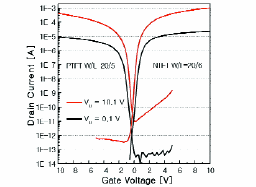
FIGURE 1 — Typical transfer characteristics of SLS poly-Si TFTs.
Comparison of some characteristics of thin-film-electroluminescent ZnS:Er,F planar and edge emitters
Nataliya A. Vlasenko
Pavel F. Oleksenko
Ludmila I. Veligura
Miroslav O. Mukhlyo
Zinaida L. Denisova
Viktor F. Zinchenko
National Academy of Sciences, Ukraine
Abstract — The following main differences have been revealed in the characteristics of an edge thin-film-electroluminescent ZnS:Er,F emitter compared to those of a similar planar emitter: (1) the 1.535-μm band more highly dominates over other bands in the EL spectrum; (2) the voltage (V) dependence of the intensity of this band is the strongest; (3) the 1.535-μm band narrows with increasing voltage and its frequency. The above differences are explained, firstly, by smaller optical losses in the ZnS:Er,F film for the near-infrared emission than for the visible one and, secondly, by an optical amplification over the 1.535-μm band in the edge emitter.
It is known that thin-film-electroluminescent (TFEL) structures of a MISIM type, where S is a semiconductor EL film, I is an insulator layer whose refractive index is lower than that of the EL film, M is an electrode, represents an optical planar waveguide. Therefore, most of the emission in such a structure is laterally transmitted due to the total internal reflection on the S–I interfaces and exits through the edge of the structure. This had been used to create edge TFEL emitters with a high luminance. However, the effective length of the edge emitters for the visible light is low (£1 mm) because of rather high optical losses resulting from scattering of light on grain boundaries in a polycrystalline EL film and from absorption of the light by various lattice defects.
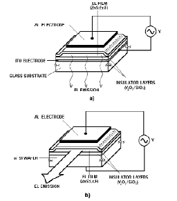
FIGURE 2 — Schematic view of ZnS:Er,F TFEL planar (a) and edge (b) emitters.
Ferroelectric properties of LC systems including chiral dopants with different molecular structure
Nataliya I. Shkolnikova
Lidiya A. Kutulya
Tatyana G. Drushlyak
Nikolay S. Pivnenko
Ekaterina V. Popova
Evgene Yu. Kopeychenko
National Academy of Sciences, Ukraine
Abstract — New ferroelectric liquid crystals (FLCs) on the basis of the eutectic mixture of phenylbenzoate derivatives including chiral components (CCs) with a different number and position of carbonyl groups in their molecular core have been investigated. The ferroelectric characteristics such as the spontaneous polarization, smectic tilt angle, rotational viscosity, and repolarization time as well as their concentration dependences are analyzed. On the basis of the previous and obtained results, the influence of peculiarities of the molecular structure of CCs on mentioned properties of FLCs are generalized.
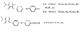
The derivatives of 1R,4R-p-menthan-3-one as components of induced FLCs belong to chiral dopants of the second type according to the classification. In their molecular structure, two chiral centers and carbonyl groups resulting in an effective transverse dipole moment are an integral part of the rigid core. In this work, new non-mesogenic arylidene derivatives of 1R,4R-p-menthan-3-one (E-isomers) were used to trace the effect of the number and position of carbonyl groups and their general contribution to the total dipole moment as well as the length of the terminal substituent in CC molecules on the ferroelectric properties of LC systems. Data for CCs are given for comparison.
Efficient and simple methods for display tone-response characterization
Raja Bala
R. Victor Klassen
Karen M. Braun
Xerox Innovation Group
Abstract — Color characterization is an important step towards achieving accurate color on displays. The characterization process typically uses colorimetric or spectrophotometric instruments to measure displayed colors, and relates these to digital values driving the device. Such measurements can be impractical for consumer applications. This paper presents two techniques for characterizing a display's tone response with no colorimetric or spectrophotometric measurements. The first is a visual technique applicable to devices that exhibit a "gamma" response, such as the cathode-ray tube. The novelty lies in the replacement of the standard luminance matching with gray-balancing for the blue channel. This approach substantially reduces observer variation in the gamma estimates for the blue channel. The second technique is applicable for the more general case of devices that do not conform to the gamma response, such as LCDs. The visual task is augmented with a consumer digital camera used as a color-capture device. The camera tone response is first characterized via a visual task. The characterized camera is then treated as a colorimeter and used to generate a tone-response characteriza-tion for the display. Experiments conducted on projection displays demonstrate that satisfactory quality can be achieved while eliminating the need for costly and tedious measurement.
Our visual method of determining the gamma for the blue primary is based on the insight that accurate gamma estimation for blue is important not for luminance reproduction, but for proper color balance, most importantly gray balance. Thus, it makes sense to use gray balancing, rather than luminance matching, as the criterion for selecting the blue gamma value. Our notion of neutral is somewhat affected by the white point of our adapting environment, so providing a reference white helps.
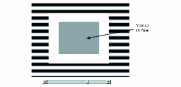
FIGURE 3 — Test field for blue gamma determination using gray balancing. The user adjusts the slider until the patch in the middle appears neutral "gray" with respect to the surround. The slider controls the digital value of the blue channel.
Selection of nanostructures for porous field-emission display
Victor P. Mammana
Vitor R. Hering
Alexandre C. Paulo
Thebano E. A. Santos
Marcelo R. Thielo
Suelene S. Mammana
Daniel den Engelsen
Alaide P. Mammana
Centro de Pesquisas Renato Archer DMI
Abstract — This paper describes the evaluation of nanostructures to be integrated into porous field-emission displays (pFEDs), based on a multilayer of copper and polyimide, pierced by holes. The evaluation work is based on diode-mode measurements performed with carbon nanotubes and nanostructured copper oxide samples obtained through wet chemical processes. A special characterization tool, based on the curve method, was used to obtain current vs. field characteristics in a repetitive and reproducible method. Histograms of threshold fields for 46 samples are presented, allowing for a comparison between different methods of nano-structure formation, which shows that carbon nanotubes yield a threshold field which is at least five times smaller than that for copper oxides.
Figure 6 shows an image obtained from a multilayer copper structure using electrophoretically deposited CNTs, which was the selected nanostructure for pFED because it combined the advantages: relatively low threshold field and a convenient deposition method. For this image, the following conditions were reached: 150 V at the gate and 3000 V at the anode for a cathode-gate distance of 37 μm. Further, gate-voltage reduction is possible by simply using thinner dielectrics between the cathode and gate. Polyimide layers as thin as 6–10 μm are commercially available, allowing substantially lower gate voltages.
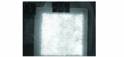
FIGURE 6 — Photo of a pFED structure operating in triode mode. This prototype is operating inside a vacuum chamber at 4 x 10⁻⁴torr. The emission area is 50 x 50 mm2. Carbon nanotubes where used as electron sources. The pixels are at the same voltage level, and no individual ballast resistance is present.
A study on reducing image-sticking artifacts in wide-screen TFT-LCD monitors
Yongeun Park
Suki Kim
Eungsang Lee
Korea University
Abstract — In order to improve the image quality of flat-panel displays, the image retention of a display has to be reduced. But at the same time, display devices also have to produce durable images while they are used for long periods of time in a single session. To achieve high-quality images with reduced image sticking in TFT-LCD devices, their voltage-holding ratio (VHR) have been increased. This technology ensures the achievement of durable images over long periods of time and also reduces the image-sticking problem. There are many ways to achieve increased VHR. In terms of the characteristics of the TFT devices, reducing the leakage-current effects is the most frequently applied method in the display industry.
It is well known that ions trapped in thin films under residual DC voltage is the cause of image sticking after application of an external DC voltage. For LC cells, another factor is the VHR. In order to increase the VHR, a storage capacitor is placed parallel to the pixel electrode to hold the pixel voltage. The parasitic capacitive coupling reduces the pixel voltage because of the gate voltage swings (kickback). Ionic impurities in the LC material also could bring about artifacts such as line image sticking that is different from the usual pictorial image-sticking artifacts. Lastly, in a silicon TFT panel, the main cause of VHR reduction is the voltage drop induced by the kickback (feed-through) when the gate voltage of the TFT changes from a high to a low gate voltage.
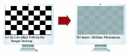
FIGURE 1 — Image-sticking phenomena.
Mechanisms for on/off currents in dual-gate a-Si:H thin-film transistors using indium-tin-oxide top-gate electrodes
Chung-Yu Liang
Feng-Yuan Gan
Fon-Shan Yeh
Ting-Chang Chang
AU Optronics Corp.
Abstract — Two types of dual-gate a-Si:H TFTs were made with transparent indium-tin-oxide (ITO) top-gate electrodes of different lengths to investigate the static characteristics of these devices. By changing the length of the ITO top gate, the variations in the on-currents of these dual-gate TFTs with dual-gate driving were found to be due to the high resistance of the parasitic intrinsic a-Si:H regions between the back electron channel and the source/drain contact. In the off-state of the dual-gate-driven TFTs, the Poole–Frenkel effect is also enhanced due to back-channel hole accumulation in the vicinity of the source/drain contact. Furthermore, we observed for the first time that under illumination the dual-gate-driven a-Si:H TFTs exhibit extremely low photo-leakage currents, much lower than that of single-gate-driven TFTs in a certain range (reverse subthreshold region) of negative gate voltages. The high on/off current ratio under backside illumination makes dual-gate TFTs suitable devices for use as switching elements in liquid-crystal displays (LCDs) or for other applications.
In our experiment, instead of top metal gate electrodes, the transparent material indium tin oxide (ITO) is patterned on top of a passivation layer. This is used as the top-gate electrodes of BCE dual-gate TFTs. The fabrication process is fully compatible with the conventional BCE TFT fabrication process and requires no extra masking steps. We fabricated two types of dual-gate TFT device structures with four various lengths for the ITO top gates on the TFT passivation layer to investigate the characteristics of dual-gate TFTs, both under dark and backside illumination conditions.
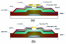
FIGURE 1 — The dual-gate a-Si:H TFT structures: (a) dual-gate TFT with source/drain and an ITO top gate overlapping (type-A). (b) Dual-gate TFT with ITO top gate centered without overlapping with the source/drain contact (type-B).