A preview of the papers appearing in the May 2007issue of the Journal of the SID. To obtain access to these articles on-line, please go to www.sid.org
Edited by Aris Silzars
Development of 100-in. TFT-LCDs for HDTV and public-information-display applications
H. C. Jin
I. B. Kang
E. S. Jang
H. M. Moon
C. H. Oh
S. H. Lee
S. D. Yeo
LG.Philips LCD
Abstract — LCDs have achieved a full-high-definition resolution of 1920 x 1080 (16:9), 600-nit brightness, 3000:1 dynamic contrast ratio, 92% color gamut, 178° viewing angle, and 5-msec response time at all gray levels and are targeted for HDTV and public-information-display applications. Some unique technologies, such as Cu bus line, advanced wide view polarizer, and wide-color-gamut lamp, were applied. A new stitching-free technology was developed to overcome the size limitation of the photomask in both the TFT and color-filter processes. The size of the panel (100 in.), based on the wide format (16:9), is determined by the maximum efficiency of the world's first seventh-generation line (glass size, 1950 x 2250 mm) in LG.Philips LCD's (LPL) Paju display cluster. The issues facing 100-in. TFT-LCDs will be discussed.
A multi-shot technology was applied to both the color filter and TFT substrate by using a new compensation method. Second, the well-known Super IPS technology was used as a wide-viewing-angle platform. To achieve better contrast ratio along the diagonal direction, we applied an advanced wide view polarizer and called it Advanced Super IPS. Third, fast response time was achieved by the combination of an ODC (over driving circuit) and newly blended low-viscosity LC (liquid crystal). Fourth, to minimize signal delay, copper-gate and bus-line technologies were adopted.
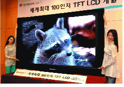
FIGURE 6 — The world's largest TFT-LCD panel (100 in.).
Mura-detection method by using a slit-beam ellipsometer
Hideyuki Murai
Koichi Ekawa
Jun Takashima
Hitoshi Naito
Nobuo Nakatsuka
OMRON Corp.
Abstract — A slit-beam ellipsometer which performs sensitive mura detection of thin films on transparent substrates has been developed. Mura is a Japanese term which means the non-uniformity of the thin-film thickness, the dielectric constant, etc. The mura thickness of polyimide films and the mura thickness of the surface of polyimide films caused by rubbing along a 30-mm-long slit beam was observed. This ellipsometer only detects the reflected light from the rubbed polyimide films onto the transparent substrates. As a result, sensitive mura detection is achieved. The slit beam generated by a cylindrical lens is irradiated onto a sample. The reflected light from the sample becomes collimated light passing through another cylindrical lens and is detected by a 2048-pixel CCD liner sensor. In addition, the in-line use of a slit-beam ellipsometer was examined. When the slit-beam ellipsometer is set up during the rubbing process, the optimum set up, where rubbing mura-detection becomes highly sensitive, was determined.
Figure 4 shows a schematic of the optical system of the slit-beam ellipsometer, which can detect mura along the reflecting points without detecting the reflected light from the back surface of the transparent substrate. The slit-beam ellipsometer is a rotating-compensator ellipsometer. It utilizes a laser diode (wavelength is 650 nm) as the incident beam, and the incident angle is set at 50°. The slit beam generated by a cylindrical lens is irradiated onto a sample.
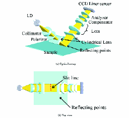
FIGURE 4 — Schematic of the optical system of the slit–beam ellipsometer.
Low-power and small-area holding latch with level-shifting function using LTPS TFTs for mobile applications
Jung-Hwan Choi
Yong-Jae Kim
Soon-Sung Ahn
Oh-Kyong Kwon
Hanyang University
Abstract — A holding latch having a level-shifting function fabricated by using a low-temperature polysilicon (LTPS) process with a 5-μm design rule on a glass backplane for power and cost effectiveness has been proposed. The layout area and the power consumption of the proposed circuit are reduced by 10% and 52%, respectively, compared with those of a typical structure which combines a static D-latch and a cross-coupled level shifter for a 2.2-in. qVGA TFT-LCD panel.
The proposed circuit is basically a holding latch which contains a level-shifting function using a capacitive-coupling effect. This circuit uses two inverters to store data similar to a conventional D-latch. The proposed circuit has 12 TFTs and one capacitor; therefore, it has an advantage in layout area for two reasons. First of all, to reduce the short-circuit current of the level shifter, the size of the TFTs in our proposed circuit is smaller than that of TFTs in the conventional structure. Secondly, the proposed circuit uses minimum-sized TFTs except for the P2 and N3 TFTs and is combined with the circuits. In addition, only five TFTs are connected to power lines in the proposed circuit.
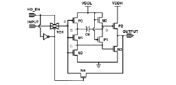
FIGURE 2 — Schematic diagram of the proposed circuit.
Development of rapid thermal processor for large-glass LTPS production
Dong Hoon Shin
Hyoung-June Kim
Hongik University
Abstract — A field-enhanced rapid-thermal-processor (FE-RTP) system that enables LTPS LCD and AMOLED manufacturers to produce poly-Si films at low cost, high throughput, and high yield has been developed. The FE-RTP allows for diverse process options including crystallization, thermal oxidation of gate oxides, and fast pre-compactions. The process and equipment compatibility with a-Si TFT manufacturing lines provides a viable solution to produce poly-Si TFTs using a-Si TFT lines.
An important advantage of the FE-RTP process is the quality of the metal-induced crystallization (MIC) poly-Si. Figure 4 shows a comparison of the microstructures of MIC poly-Si at 600 and 750°C. The apparent structure is composed of Ni silicide networks which are formed after impingement of MIC lateral growth. High-temperature results in a large silicide network with a low number density of silicides. Because the Ni silicide acts as a source of leakage current, high-temperature MIC results in superior TFT characteristics with low leakage current.

FIGURE 4 — Optical micrographs showing the microstructure of MIC poly-Si.
Electronic structure and electrical conductivity of MgO protecting layer in plasma-display panels: A tight-binding quantum chemical study
Akira Miyamoto
Hiromi Kikuchi
Hiroaki Onuma
Hideyuki Tsuboi
Michihisa Koyama
Nozomu Hatakeyama
Akira Endou
Hiromitsu Takaba
Momoji Kubo
Carlos A. Del Carpio
Tohoku University
Abstract — The tight-binding quantum chemical molecular dynamics code, Colors, has been successfully applied to the electronic-structure calculations of the MgO-protecting-layer model in plasma-display panels (PDPs). The code succeeded in reproducing the band-gap energy of the MgO crystal structure. The energy gap between the bottom of the conduction band (CB) and the top of valence band (VB) was 7.45 eV, which is in quantitative agreement with the experimental and previous theoretical results. The electronic structure of the undoped MgO model and Si-doped MgO model was also calculated. The impurity level was 2.15 eV lower than that for the bottom of the CB. This result was in qualitative agreement with recent cathodoluminescence measurements. In addition, we have already succeeded in developing a novel electrical conductivity simulator using the spatial distribution of the probability density of wave functions obtained from the tight-binding quantum chemical molecular dynamics code, Colors. The electrical conductivity of the MgO-protecting-layer model was estimated with and without an oxygen defect and a significant change in the electrical conductivity of the MgO-protecting-layer materials was observed with the introduction of oxygen defects.
To develop improved MgO protecting materials, it is important to advance the understanding of the electronic structures of the MgO protecting materials, which seems to be difficult by performing only experimental methods. A quantum chemical calculation based on the density functional theory (DFT) is one of valid tools to determine the details of the electronic structure of the materials. However, it requires an extremely large computational cost and impedes the use of a large-scale model which is essential in taking into account the dopant(s). From an engineering point of view, it is indispensable to develop a more effective method which will enable the use of a large-scale model.
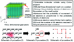
FIGURE 1 — Schematic of computation flow in the present electrical conductivity simulator.
Influence of sustaining frequency on the production efficiency of excited Xe atoms studied in unit cell microplasma for ACPDPs using spectroscopic diagnostics
Jun-Seok Oh
Osamu Sakai
Kunihide Tachibana
Kyoto University
Abstract — The effects of the driving frequency of the sustaining-voltage pulses on microplasmas in a cell of an ac plasma-display panel (ACPDP) were investigated using spectroscopic diagnostics [optical emission spectroscopy (OES) and laser-absorption spectroscopy (LAS)]. The unit discharge cell has a structure similar to that of a general commercial ACPDP, but it is prepared for three-dimensional (3-D) observation using a pair of micro-prisms. When the near-IR emission by OES and the absorption signal by LAS were observed in the front and side views simultaneously, it was determined that the discharge was concentrated at the center of the discharge space and quickly responded to an applied electrical potential as the sustaining frequency increases. The production efficiency of excited Xe**(2p) atoms and vacuum-ultraviolet (VUV) photons, which was estimated from the spectroscopy results with the measured power dissipated in the discharges, increased as the frequency of the sustain pulses increases to 100 kHz. At 250 kHz, however, the efficiency remarkably decreased because of an inefficient time for excimer formation and, possibly, for wall-charge formation. From the quantitative analysis of the efficiency, the most-efficient frequency for the sustain voltage was around 100 kHz in the case of Xe(5%)–Ne at 500 Torr, i.e., the efficiency depended on both the priming particles [excited Xe*(1s5) atoms] in space and the charged particles on the dielectrics.
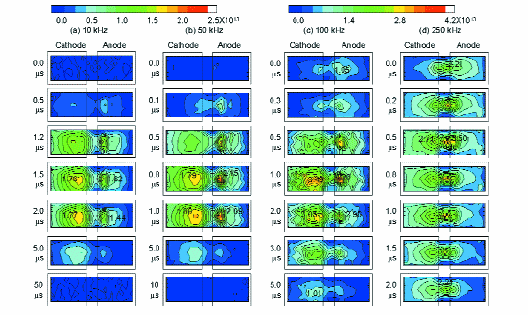
FIGURE 6 — Spatiotemporal behaviors of metastable Xe*(1s5) atom density (in units of 1013 cm–3) at (a) 10 kHz, (b) 50 kHz, (c) 100 kHz, and (d) 250 kHz at a sustaining voltage of 210 V in a half cycle where the left side is working as the cathode and the right side as the anode.
Depth- and viewing-angle-enhanced 3-D/2-D switchable display system with high contrast ratio using multiple display devices and a lens array
Heejin Choi
Yunhee Kim
Joohwan Kim
Seong-Woo Cho
Byoungho Lee
Seoul National University
Abstract — An improved 3-D/2-D switchable display system with enhanced depth and viewing angle by adding two LCD panels to an integral imaging system has been realized. The proposed system uses the see-through property of an LCD panel and displays multiple sets of elemental images on the LCD panels to integrate them on multiple locations simultaneously. As a result, the depth of the 3-D image can be enhanced. For wide viewing angles, the time-multiplexing method was adopted by displaying mask patterns on the front LCD panel. In addition, another technique to increase the contrast ratio of the proposed system has also been developed. Some experimental results will be provided.
The structure of the proposed method is shown in Fig. 4, where the system is composed of a lens array, two LCD panels, and a display device. The display device and LCD panel 2 are located around the focal length f of the lens array as shown in Fig. 4, and the proposed system can form real and virtual 3-D images simultaneously and increase the total depth significantly by using this configuration. LCD panel 1 is located directly in front of the lens array. In the 3-D mode, both the depth and the viewing angle of the 3-D images are enhanced.
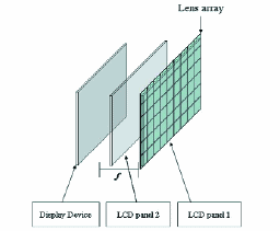
FIGURE 4 — The structure of the proposed system.
Spatial optical modulator (SOM): Samsung's light modulator for next-generation laser displays
Sang Kyeong
Yun et al.
Samsung Electro-Mechanics Co., Ltd.
Abstract — A new type of diffractive spatial optical modulators (SOMs) has been developed for projection-display and other applications such as holographic data storage, programmable lithography, and optical communications. It exhibits the inherent advantages of fast response time and high-performance light modulation, suitable for high-quality and high-resolution projection displays. The ±1st-order efficiency and contrast ratio of 39% and 1000:1 was achieved for a prototype SOM. The response time can be as fast as 0.7 μsec with a 400-nm displacement, enough to make a full-HD display, being driven by 10 V. A laser display in full-HD format (1920 x 1080) was successfully demonstrated by using prototype projection engines having SOM devices, signal-processing circuits, and projection optics.
A simplified optical schematic diagram of the display's single color channel is described in Fig. 2. The light source can be an optically pumped semiconductor laser (OPSL) based on a vertical external cavity surface-emitting laser (VECSEL) as well as a single laser diode (LD) or LD array. By using an LD, a pair of collimator–cylinder lenses are needed to form on the SOM a linearly focused light beam which after reflection is divided into two symmetrical +1st and –1st diffraction orders. These orders pass through a projection lens. Schlieren stop and reflecting light from a scanning mirror approach the screen where the SOM array magnified image is reconstructed.
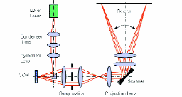
FIGURE 2 — Conceptual optical diagram of the SOM–based projection displays.