A preview of the papers appearing in the August 2007 issue of the Journal of the SID. To obtain access to these articles on-line, please go to www.sid.org
Edited by Aris Silzars
Design of large-area OLED displays utilizing seamless tiled components
Mark Aston
TEW Engineering, Ltd.
Abstract — In recent years, the majority of R&D for large-area displays has been to serve the production of large monolithic substrate technology such as plasma-display panels (PDPs) and TFT-LCDs. While the pursuit of large displays for domestic and light-industrial use benefits from the production of these high-quality high-pixel-count technologies, there is still a need to produce displays in formats other than 4:3 or 16:9 and on a larger scale than currently available in single-substrate displays. The options that exist for producing tiled displays from emerging technologies is examined and a practical technique for creating large-area (1.8 x 1.2 m and larger) monochrome or color displays from tiling smaller units is discussed. This presents a cost-effective approach for arranging small tiles to create a much larger screen and offers a simple way to address the market gap between large monolithic displays and small conventional LED video-wall displays in the size range of 1–10-mm pixels for advertising and industrial use. By examining the requirements for pixel size and pitch against the range of viewing distances commonly associated with the target markets for these displays, it will be shown that complex manufacturing is not always required.
The overlapping aspect of the tiles must be constrained to give a continuous appearance to the display, and the compound angle at which the criteria no longer can be met is defined from the arrangement of tiles illustrated in Fig. 8. The glass which contains the OLED is transparent (due to the advent of glass encapsulation) and thus the edge of one active display area lies immediately adjacent to the active display areas of the surrounding tiles.
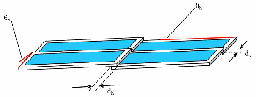
FIGURE 8 — Configuration of the compound angle of an OLED tile to allowing seamless tiling. dh is the overlap in the horizontal direction (equivalent to the edge of tile to edge of active area distance along tile length). dv is the overlap in the vertical direction (equivalent to the edge of tile to edge of active area distance along tile width). θh is the horizontal angle of a tile from the display plane, P. θv is the vertical angle of a tile from the display plane, P.
An active-matrix organic light-emitting-diode pixel circuit for the compensation of I x R voltage drop in power line
Sang-Hoon Jung
Hong-Koo Lee
Tae-Joon Ahn
Chang-Yeon Kim
Chang-Dong Kim
In-Jae Chung
LG.Philips LCD
Abstract — A new voltage-driving active-matrix organic light-emitting-diode (AMOLED) pixel circuit is proposed to improve the display image quality of AMOLED displays. Because OLEDs are current-driven devices, the I x R voltage drop in the power lines is evitable. Accordingly, the I x R voltage-drop compensation scheme should be included in the pixel-driving method when a voltage-compensation method is used. The proposed pixel was designed for the compensation of an I x R voltage drop in the power lines as well as for the compensation of the threshold-voltage non-uniformity of low-temperature polycrystalline-silicon thin-film transistors (LTPS TFTs). In order to verify the compensation ability of the proposed pixel, SPICE simulation was performed and compared with those of other conventional pixels. When the Vss voltage varies from 0 to 1 V, the drain current of the proposed pixel decreased by under 1% while that of conventional Vth compensation methods without Vss compensation decreased by over 60%. 2.2-in. QCIF + full-color AMOLED displays, which employ the proposed pixel, have been also developed. It was verified by comparison of the display image quality with a conventional panel that our proposed panel successfully overcame the voltage-drop problems in the power lines.
Display images of the proposed 2.2-in. AMOLED panel along with those from a conventional one are shown in Fig. 6. Figure 6(a) is an image from a conventional panel that cannot compensate for the voltage rise in the Vss line, but can only compensate the Vth of the driving TFT. The luminance variation due to TFT non-uniformity was not easily observed, but the luminance was reduced by 16% from side to center. The proposed panel, which is able to compensate for the voltage drop in the power lines, exhibited improved luminance uniformity from side to center as shown Fig. 6(b).
FIGURE 6 — The display image of the 2.2-in. panels. (a) A panel employing Vth compensation without Vss compensation; (b) and (c) a panel employing the proposed pixel with Vth and Vss compensation.
Novel a-Si:H TFT pixel circuit for electrically stable top-anode light-emitting AMOLEDs
Juhn Suk Yoo
Hojin Lee
Jerzy Kanicki
Chang-Dong Kim
In-Jae Chung
LG.Philips LCD
Abstract — A novel pixel circuit for electrically stable AMOLEDs with an a-Si:H TFT backplane and top-anode organic light-emitting diode is reported. The proposed pixel circuit is composed of five a-Si:H TFTs, and it does not require any complicated drive ICs. The OLED current compensation for drive TFT threshold voltage variation has been verified using SPICE simulations.
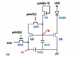
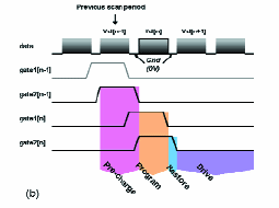
FIGURE 2 — (a) Schematic diagram of the proposed circuit and (b) timing diagram of data signal and gate control signals. The proposed pixel circuit operates in four stages; pre-charge, program, restore, and drive.
Switchable helical holographic structures
Suraj P. Gorkhali
Gregory P. Crawford
Maryna Yemtsova
Theo Rasing
Brown University
Abstract — A 3-D array of helical structures fabricated using holographic polymer-dispersed liquid crystals (H-PDLC) is presented. Multiple coherent beams are interfered to create a constructive helical pattern which is permanently captured using the standard H-PDLC method. Films with such an array of helical structures have both diffractive and circular polarization sensitive reflective properties. Iso-intensity patterns, design parameters, fabrication process, and optical/electro-optical performance of these periodic helical structures are discussed along with their potential application for advanced electro-optical devices.
The regular arrangement of helical posts in a hexagonal pattern results in a two-dimensional diffraction grating, thus a fraction of the transmitted light is diffracted. The diffraction pattern produced by a normally incident argon-ion laser (351 nm) is shown in Fig. 4(a). There are six first-order diffraction spots at a cone angle of 25° when probed with a 633-nm laser which is in agreement with the arrangement and separation of the helical posts separation mentioned above. Broadband focused white light is also diffracted and dispersed into six bright spectra shown in Fig. 4(b). The 2-D Fourier transform of the hexagonally patterned helical structure shows six discrete sharp peaks matching the diffraction pattern [Fig. 4 (inset)].
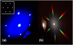
FIGURE 4 — (a) Diffraction pattern from argon-ion laser at 351 nm and (b) broadband focused white light. 2-D Fourier transforms along the XY plane illustrating the expected diffraction pattern (inset).
Patterned liquid-crystal laser film for multi-dimensional multi-color emissive film technology
Scott J. Woltman
Gregory P. Crawford
Brown University
Abstract — A two-dimensional array consisting of dye-doped reflection-mode holographic-polymer-dispersed liquid crystal (H-PDLC) lasers with alternating pitch lengths is presented. These post structures each reflect at a narrow bandwidth of light. The addition of laser dye to the H-PDLC system allows for the generation of laser emission at the edge of the reflection band, or photonic band gap. In patterning these H-PDLC post structures, a narrow-linewidth patterned emissive color film is realized. The potential of such films and their implication in the display industry is discussed. In creating a three-color array, an active emissive color film could replace the backlight and color-filter components within the display. Such a patterned system would possess a wide color gamut, through spatial color synthesis, formed by narrow-linewidth lasing structures with well-defined wavelengths of emission.
These lasing arrays hold promise as emissive color films for display applications, as illustrated in Fig. 1. In making use of a three-color laser array pumped with a flashlamp, a union of the backlight and color filter are realized. Whereas a typical backlight/color-filter combination in an LCD are used to eliminate unwanted portions of the spectrum for each subpixel, each subpixel of the lasing color film emits only over a small range of wavelengths (<10 nm), eliminating the need for the high-intensity backlight currently used in LCDs and color filters with efficiencies of no greater than 33%.
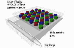
FIGURE 1 — An illustration of an array of lasing H-PDLCs, comprised of "posts" with different pitch lengths for use as a backlight for an LCD. A flashlamp is used to induce lasing from the film.
Wide-angle film diffuser
Zhijian Z. J. Lu
James W. Lee III
Jong Man Kim
Pekoma, Inc.
Abstract — A unique roll-to-roll mass-producible high-transmission wide-angle diffuser (WAD™) film for use in LCD backlights is reported. WAD™ diffuser films include optical structures that efficiently manage forward light scattering and significantly reduces backward light scattering. WAD™ technology facilitates backlights with significantly higher brightness and thinner backlight profiles.
The backscattering from a WAD™ diffuser has been investigated and it was compared to that from bead diffusers. Figure 3 shows photographs taken from the back side of a WAD™ diffuser and a high-grade bead diffuser illuminated with a collimated He–Ne (633 nm) laser beam. The observed light in the backward direction for a WAD™ diffuser is mainly specular reflection from the interface of air and the back side of the diffuser. In contrast, strong backward scattering is readily visible in the case of a bead diffuser. The low backscattering from a WAD™ diffuser is further evidenced by the high total transmission as measured using ELDIM EZ Contrast. The total transmitted (direct and diffused) light by the WAD™ diffuser is 56% higher than that of a high-grade bead diffuser.
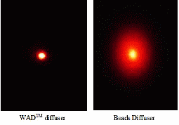
FIGURE 3 — Photographs of backscattering from WAD™ and bead diffusers.
Mathematical modeling of the LCD response time
Pierre Adam
Pascal Bertolino
Fritz Lebowsky
GIPSA-Lab, INPG-CNRS
Abstract — Techniques to reduce LCD motion blur are extensively used in industry and they depend on an inherent LCD parameter: response time. However, normative response time is not a sufficient reference to improve LCD performance and all the gray-to-gray response-time quantities are required to obtain good improvement. However, measuring and gathering all the gray-to-gray transitions takes an excessive amount of time. Consequently, we propose a novel LCD model to simulate as well as compute gray-to-gray transitions (response time and behavior) from a reduced measurement set in order to decrease the response-time measurement.
Figure 6 shows the superposition of the actual measurements: one transition from ↑T0 (L0128) and three transitions from ↑T* (L32128, L64128, L96128). According to this relationship, we can deduce the LC behavior of any transitions of ↑TY (with Y ¹ 0), from the curve of the transition L0Y.

FIGURE 6 — Superposition of measured transitions L32128, L64128, and L96128 over L0128.
Tailored liquid-crystal switching on ferroelectric polymer films
Hemang J. Shah
David Delaine
Adam K. Fontecchio
Drexel University
Abstract — The development of voltage-controlled visible-wavelength progression in displays and optical data storage devices using ferroelectric polymers and liquid crystals is described. Ferroelectric polymers are materials that have a ready distribution of dipoles which can be oriented by manipulating material composition and external fields. Utilizing the charge polarization distribution, their performance as an alignment layer for inducing liquid-crystal alignment is presented. The switching response of the devices was tailored by changing the material composition through copolymers and nanoclay doping.
Using PVDF-based polymers as an alignment layer, an analog display is developed where controlling the magnitude of the applied electric field generates the desired wavelength of light. Conventional LCDs generate a desired color in a pixel through the use of three subpixels, corresponding to red (R), green (G), and blue (B) wavelengths. The R, G, and B components are added additively to generate the desired color. Through PVDF-LC devices, every pixel can be designed to generate the desired colors allowing an increase of 300% in the resolution of the commercial displays.
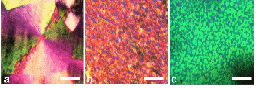
FIGURE 3 — Polarized optical images of LC alignment on (a) PVDF film, (b) PVDF–Nanoclay film, and (c) P(VDF-CTFE)–Nanoclay film. The scale bar on all images represents 50 μm. The blue spots in (b) and (c) are the clay aggregates.
Chiral SmA* materials for display applications?
David M. Walba, Eva Korblova,
Lior Eshdat, Michael C. Biewer,
Hong Yang, Christopher Jones,
Michi Nakata, Mara Talarico,
Renfan Shao, Noel A. Clark
University of Colorado
Abstract — The potential of chiral SmA* materials for electro-optics applications exploiting the electroclinic effect will be explored. In this context, the nature of the de Vries smectics will be discussed, and characterization and application of some rare SmA* materials exhibiting a large and relatively temperature-insensitive electroclinic coefficient will be described.
Since the first description of the electroclinic effect in chiral smectic A (SmA*) liquid crystals (LCs) by Meyer and Garoff, this fast analog electro-optic (EO) effect seemed to hold great promise for information-display applications. The electroclinic effect has been under utilized, however, due to several problems. Chief among these is the formation of visible stripes in the cell in the presence of an applied field, due to tilt-induced layer shrinkage. In addition, the predicted and observed strong temperature dependence of the electroclinic coefficient (χ º optic axis tilt per unit applied field) is highly problematical for display applications.
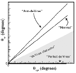
FIGURE 1 — Illustration of the relationship between θopt, θxr, and the de Vries character.
Polarization-independent modulation for projection displays using small-period LC polarization gratings
Ravi K. Komanduri
W. Michael Jones
Chulwoo Oh
Michael J. Escuti
North Carolina State University
Abstract — Progress in the use of liquid-crystal polarization grating (LCPG) to modulate unpolarized (and polarized) light with a grating period as small as 6.3 μm is reported. Similar to LCPGs formed at larger periods (11 μm) reported previously, polarization-independent switching, predominantly three diffraction orders, maximum contrast ratios of ~100:1 for unpolarized broadband light, very low scattering, and diffraction efficiencies ≥98% continue to be observed. The smaller period led to an expected lower threshold voltage, even though the thickness was greater. Because the smaller grating period enables a brighter result from a Schlieren projection scheme for a microdisplay using the LCPG light valve, the inherent tradeoffs involved with both material and design parameters are discussed, and prospects for a polarization-independent projection display are commented upon.
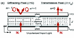
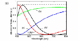
FIGURE 1 — LCPG properties. (a) Side view of the pixel structure in its diffracting and transmissive states and (b) raw transmittance of the zero order with input unpolarized light.
Carbon nanotubes and semiconductor nanowires for active-matrix backplanes
D. Pribat
C. S. Cojocaru
M. Gowtham
L. Eude
P. Bondavalli
P. Legagneux
LPICM, Ecole Polytechnique
Abstract — Carbon nanotubes and semiconductor nanowires are a new class of materials currently being studied within the context of molecular electronics. Because of their excellent characteristics, transistors based on carbon nanotubes and semiconductor nanowires could become the workhorse of the post-CMOS era. Since carbon nanotubes as well as Si or Ge nanowires can be grown at low temperature, using similar CVD-type processes and on non-crystalline and non-refractory substrates, they could (and will) certainly be used in the near future for the fabrication of thin-film transistors and active-matrix backplanes. However, the development of these nanomaterials is hampered by the general problems posed by their manipulation, placement, and in-plane organization. The possible use of CNT random networks (that do not need to be organized) and the fabrication of thin-film transistors will be reviewed. Then a new way of organizing semiconductor NWs in a thin-film transistor, based on the use of lateral porous anodic alumina templates, will be presented.
Figure 5 shows a preliminary result of Si nanowire (NW) growth in a lateral anodic alumina membrane. The vapor-liquid-solid (VLS) growth has been performed at 550°C with a mixture of 5% SiH4 diluted in H2 at a total pressure of 5 mbar for a 100-sccm total flow. Clearly, the process is not yet uniform and only few NWs emerge from the lateral membrane. Also, parasitic Si deposition is apparent, which means that the H2 decomposition rate (which supplies atomic hydrogen) at the growth temperature is too low.
FIGURE 5 — Growth of Si NWs in a lateral porous alumina membrane. (a) View of the membrane and SiO2 cap, with some NWs emerging. (b) Close-up view of an emerging NW.
Fast phase modulation using dual-frequency nematic liquid crystals
Mikhail I. Barnik
Serguei P. Palto
Shubnikov Institute of Crystallography
Abstract — Experimental study and numerical simulations of optical phase modulators based on nematic liquid crystals characterized by frequency sign inversion of the dielectric anisotropy has been performed. The received results point out an extreme role of back-flow effects and electro-hydrodynamic instability, which make restrictions for creating high-speed phase modulators with large switchable values of phase retardation. It is shown by numerical simulations that the hydrodynamic destabilization can be suppressed by decreasing the ratio of Leslie coefficients |α2/α4,5|.
Double-layer LC cells can be used to expand the dynamic range of the fast optical phase modulation. In this case, the same speed at an equivalent phase modulation range is achieved at lower values of the high-frequency voltage, when LC is not subjected to EHD instability. A double-layer cell design and its electric connection to the net source are schematically shown in Fig. 4. The cell assembly consists of three stacked glass plates with two gaps between them, which are filled by AP-99-1 LC material.
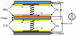
FIGURE 4 — A sketch of the double-layer liquid-crystal cell and its connection to the power source. The arrows show the rubbing directions.
Visual gamma measurement and methods to compare gamma models
Jacobus Besuijen
University of Twente
Abstract — The correct estimation of the gamma exponent describing the tone-reproduction curve of a display is an important step in color management. Several methods for visual gamma estimation have been proposed. In this study, the theoretical merits and practical problems of a number of these methods are discussed and compared, and improvements are suggested. A new method to compare gamma models with different numbers of parameters is introduced. In an experiment, spatial and temporal brightness-matching methods were tested with 32 untrained subjects working on a CRT and an LCD with different resolutions under office and low-illumination conditions. Illumination had no effect on gamma estimations. Subjects had great difficulties with spatial brightness matching at low resolutions. Temporal and spatial visual brightness matching for untrained subjects showed a larger gamma than photometric fits.
Through its years of display-market domination, the CRT has defined the standard and the tone reproduction curve (TRC) with power function form has its merits. The non-linearity of the CRT is not a deficiency but a highly desirable feature: it is very nearly the inverse of the lightness sensitivity of human vision. The non-linear TRC causes a CRT's response to be roughly perceptually uniform, this means the coding of the images during storage and transmission is nearly optimal and therefore TRCs of other display technologies are adjusted to mimic this behavior. Another advantage of the power function is that the transmission is defined by a single parameter: the exponent gamma.
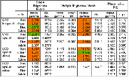
TABLE 8 — Overview of results from gamma estimation based on a single brightness match, multiple brightness matches, and photometric fits and regressions to find the equivalent single parameter gamma for two- and three-parameter models. Orange-colored background denotes a significant difference with photometric gamma, green denotes no significant difference.
Support Vector Machine (SVM) based compression artifact-reduction technique
Mainak Biswas
Sanjeev Kumar
T. Q. Nguyen
Nikhil Balram
Marvell Semiconductor
Abstract — A compression artifact-reduction algorithm based on support vector regression is proposed. The algorithm belongs to a broad family of standard reconstruction methods, but a standardization model is determined from a set of training samples of original images and the corresponding noise-corrupted version. As opposed to artifact-reduction methods specific to each type of compression artifact (e.g., blocking, ringing, etc.), we treat such artifacts as a manifestation of the same problem, which is the quantization of DCT coefficients. In the testing step, the algorithm tries to undo the effect of quantization by using the relationship between the original and artifact-corrupted image, determined during the training step. Experimental results exhibit significant reduction in all types of compression artifacts.
In transform coding, an image is represented as a linear combination of transform basis functions. Low bit rates normally require coarse quantization of transform coefficients. As a result, an image is represented by a fewer number of basis functions than necessary. The shapes of the basis functions and the way they are inter-laid become crucial to the final image quality. For non-overlapping DCT, the most common artifact is blockiness, which is due to the presence of visible discontinuities at block boundaries. An example of an image degraded by blocking artifact is illustrated in Fig. 1.
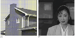
FIGURE 1 — (a) Illustration of blocking artifacts manifested due to coarse quantization of DCT coefficients. (b) Illustration of blocking and ringing artifacts on non-detailed regions and on sharp edges.