Are There Alternatives to TFTs in AMLCDs?
In an effort to further reduce manufacturing costs, several AMLCD manufacturers are developing technologies to replace the expensive TFT array. Here, several potential alternatives are examined.
by W. den Boer, G. S. Smith, W. C. Wang, L. Lin, H. Kang, S. J. Chen, and C. M. Huang
AMORPHOUS-SILICON (a-Si) thin-film-transistor liquid-crystal displays (TFT- LCDs) have been very successful as the flat-panel display of choice for many applications, from cell phones to TVs. To be profitable in this business, AMLCD manufacturers need to make large investments in state-of-the-art manufacturing facilities. Much of the investment is for the manufacture of the TFT array, which requires a four- or five-mask-step process and at least seven thin-film layers. To lower costs and further reduce process complexity, a number of manufacturers are developing new technologies. For example, a lift-off process1 and laser patterning have been proposed to eliminate the separate lithography step for the indium tin oxide (ITO) pixel, potentially leading to a three-mask process. However, the process window for large-area processes with three or four masks can be quite narrow, having an impact on manufacturability. Therefore, TFT array processes with four or fewer mask steps have not been widely adopted. This brings up the question, Are there any simpler, lower-cost alternatives to TFTs in AMLCDs?
Are There Alternatives?
The purpose of an active-matrix backplane is to accurately charge the liquid-crystal (LC) pixel to the data voltage and then sustain this voltage on the pixel until the next refresh. We believe that this can be achieved with a simpler pixel circuit and process than using a TFT. A non-linear resistor or thin-film diode (TFD) is a simpler device than a TFT and can be manufactured with only two or three mask steps and only three thin-film layers.2 TFD-LCDs, which have been on the market for more than 20 years,3 typically have one TFD per pixel, and the data lines are on the opposite substrate. In this pixel circuit, the LC capacitance is connected in series with the TFD. This has the disadvantage that any variation in the diode characteristics across the display area – with temperature or over time – will change the voltage across the LC and, therefore, the gray scale of the pixel. In addition, resistance–capacitance (RC) delays on row lines in single-diode LCDs cause brightness gradients. Single-diode LCDs, also called metal-insulator-metal (MIM) diode LCDs, have therefore been used only in small displays with a limited number of gray levels.
Willem den Boer and G. Scott Smith are with ScanVue Technologies LLC, 2721 NE Charlois Drive, Hillsboro, OR, 97124-1339; telephone 503/846-1641, e-mail: willem@scanvuetech.com. W. C. Wang, L. Lin, H. Kang, S. J. Chen, and C. M. Huang are with Wintek Corp., Taichung, Taiwan.
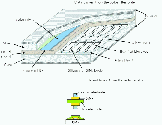
Fig. 1: Cutout view of DSD-LCD and layout/cross section of the diode.
The Dual-Select Diode (DSD) pixel-circuit configuration solves these problems. A cutout cross section of the DSD-AMLCD is shown in Fig. 1. It has two select lines for each row of pixels, connected to each pixel electrode through TFDs or non-linear resistors. The circuit with two diodes per pixel cancels out diode variations over time, with temperature, and across the display area. It also compensates for much of the RC delay on the select lines, potentially enabling large-sized displays of at least 40 in. on the diagonal.5
Similar to a TFT-LCD, the DSD-LCD is addressed one line at a time. A row of pixels is selected by applying simultaneously opposite polarity pulses of approximately +15 V and –15 V to the S1 and S2 select lines, respectively. This biases the ITO pixel electrode to a voltage (Vs1 + Vs2 )/2. At the same time, the gray-level data voltage is applied to the ITO data line on the color plate. When the select pulses are terminated, the non-linear resistors (TFDs) are no longer conducting, and the data voltage is accurately stored on the LC capacitor. Only the two diodes within the same pixel need to have close to identical current–voltage characteristics. This is normally the case because the diodes within one pixel are separated at most by only a few hundred microns and have the same film thickness, temperature, and aging history. Long-range variations of the TFDs across the display area and variations with temperature or over time have little or no impact on the gray level of the pixel. This is the result of automatic cancellation of these variations in the circuit with two diodes.
Low-Mask-Count Array Processes
The DSD active-matrix backplane can be manufactured with two or three mask steps, as shown in the diode cross sections of Fig. 1. Several non-linear conducting materials, such as silicon-rich silicon nitride (SiNx), Ta2O5, and diamond-like carbon can be used for the non-linear resistor. SiNx is particularly attractive because it can be deposited in standard plasma CVD equipment used for a-Si and silicon nitride in TFT-LCDs. In a three-mask process, the first pattern delineates the ITO pixel and bottom electrode for the diodes. Then, the SiNx layer is deposited and patterned. Finally, a metal is deposited and, withthe third mask, patterned into the select lines and top electrodes of the diodes. In a two-mask process, patterning of the SiNx and metal layers is combined into one photolithography step. It is also possible to reverse the sequence of the conductors by depositing and patterning the metal first and the ITO pixel last.
Diode Characteristics and LC Modes
In Fig. 2, the measured non-linear resistor characteristics of SiNx diodes are shown. Data are for varying x in SiNx, which is achieved by adjusting the ratio of SiH4 and NH3 gases in the plasma chemical-vapor-deposition (CVD) process. The diodes have a bottom Al electrode and a top transparent conductor ITO electrode. By varying the N/Si ratio x in the film for a diode with an area of about 10 x 10 μm, the ON and OFF current can be tailored for application as a switch in AMLCDs, i.e., the OFF current at ± 5 V should be in the picoampere range and the ON current at ± 15 V should be more than about 0.1 μA. Frenkel–Poole conduction is believed to be the physics principle responsible for the non-linear behavior.
It is interesting to note that some of the earliest developed AMLCDs used non-linear resistors (or "varistors") of ceramic ZnO as a switch at each pixel.4 One of the reasons this technology was not commercially successful was the incompatibility of opaque ceramic substrates with transmissive LCDs. Ceramic ZnO varistors have been used for a long time in surge-suppression circuitry. Recently, interest in sputtered ZnO thin films has increased after TFTs with ZnO as the semiconductor layer had been demonstrated with good performance.
However, considering its original use in electronics for non-linear resistors, can ZnO thin films be suitable as the switching material in vertical sandwich-type switches or in lateral gap-type switches for AMLCDs? If the latter is the case, a one-mask process for DSD- AMLCDs can be envisioned, in which a blanket semiconducting ZnO film is followed by a patterned transparent conductor such as ITO. The spacing of a few microns between the ITO select lines and the ITO pixel electrode would act as the non-linear resistor for the active-matrix backplane.
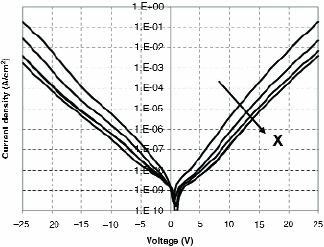
Fig. 2: Measured characteristics of SiNx diodes with varying N/Si ratio x and a SiNx thickness of 200 nm.
The configuration shown in Fig. 1 is compatible with both the twisted-nematic liquid-crystal (TN-LC) mode and also with several wide-viewing-angle LC modes, such as the multidomain vertical alignment (MVA) or patterned vertical alignment (PVA) modes. The in-plane-switching (IPS) mode can be implemented in DSD-LCDs as well by moving the data lines to the active-matrix array.
Prototype Displays
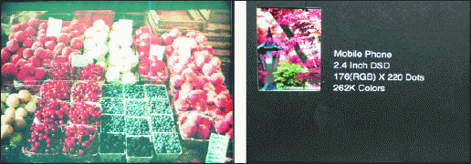
Prototype TN-DSD-AMLCDs were fabricated a number of years ago at OIS Optical Imaging Systems and recently at Wintek Corp. Images on a 10.4-in. VGA DSD prototype and a small mobile-phone DSD display are shown in Fig. 3. They have a contrast ratio exceeding 200:1 and display up to 262,000 colors. The performance, including response time, is similar to that of a TFT-LCD with the same LC fluid. In a side-by-side comparison with a TFT-LCD, the average observer does not see a difference.
Process Comparison
In Table 1, the process steps of a four-mask TFT process are compared with that of a two-mask DSD-array process.
The DSD process is much simpler and has a higher throughput and lower mask count. The total thickness of the plasma CVD layers is reduced by a factor of 8 for the DSD process as compared with the a-Si TFT process. The number of etching steps is significantly reduced as well. Design rules for DSD arrays scale with display and pixel size.5 For example, in a 30-in. display, the minimum feature size scales to 30 μm and the overlay tolerance to 10 μm, allowing the use of lower-cost patterning techniques.
A study by market-research-firm DisplaySearch7 concluded that the manufacturing cost of an LCD module based on DSD arrays can be about 20% lower than that based on a-Si TFT arrays. The difference is attributed to 60–70% lower capital investment in the array process. The study assumes that the manufacturing yield is at least as good as for a-Si TFT LCDs.
Shared Select Configuration
The circuit configuration of Fig. 1 requires two select lines for each row of pixels. The added select lines have an impact on the pixel aperture and doubles the number of row interconnects. This can be avoided by using the shared select-line circuit shown in Fig. 4. Each select line is connected through non-linear resistors to both the pixel electrodes above and below it.6
In this configuration, the opposite-polarity select pulses for each row overlap by approximately one line time. A row is selected when both adjacent bus lines are simultaneously turned on. It can be shown by circuit modeling that, with the correct polarity of the data voltages, the leakage through the diodes on a previous row is negligible when the adjacent row is selected. The shared select-line approach increases the pixel aperture and reduces the number of interconnects by eliminating 50% of the select lines.
Wintek Corp.
Fig. 3: Image on a 10.4-in. VGA prototype (left) and a mobile-phone prototype (right) DSD-AMLCD.
Table 1. Process comparison between a-Si TFT and SiNx DSD array processes
|
Process steps
|
Four-Mask a-Si TFT |
Two-Mask DSD |
| Sputter Deposition (ITO, metals) |
3 |
2 |
| Plasma CVD Deposition (a-Si, SiNx) |
4 (800 nm total) |
1 (100 nm) |
| Etching |
8 |
3 |
| Photolithography |
|
|
| Mask Count |
4 |
2 |
| Resolution |
3 or 4 μm |
>6 μm |
| Overlay Tolerance |
1 μm |
>2 μm |
Summary
Prototype DSD-AMLCDs have been demonstrated for small mobile as well as larger-sized applications. The DSD-AMLCD is fabricated with a very-low-cost active array process with only two or three mask steps and one single PECVD step with a deposition time of about 40 sec. Since the lithography and PECVD equipment account for a large part of the capital equipment expenditure in an AMLCD line, adoption of DSD technology would lead to a 60% reduction of capital investment in the array process, assuming similar yield in production as a-Si TFT arrays. For large DSD AMLCDs, the design rules scale with the pixel and display size,5 enabling a further reduction in patterning cost by the use of lower-resolution lithography, maskless patterning, or ink-jet patterning. The key to success of DSD technology will be the reproducible manufacturing of reliable non-linear resistors in a simple process with three or fewer layers and three or fewer patterning steps. Development is under way at several AMLCD manufacturers.
References
1S. S. Yoo, H. L. Cho, O. N. Kwon, S. H. Nam, Y. G. Chang, K. Y. Kim, S. Y. Cha, B. C. Ahn, and I. J. Chung, " The Fabrication of TFTs for LCDs Using the Three-Mask Process," Proc. IMID, 948-951 (2005).
2Z. Yaniv and W. den Boer, "Addressing AMLCDs with Two-Terminal Switches," Proc. EuroDisplay, 164-169 (1990).
3H. Ohshima and S. Morozumi, "An MIM LCD with Improved TV Performance," SID Symposium Digest Tech. Papers 21, 518-521 (1990).
4D. E. Castleberry, "Varistor-Controlled Liquid-Crystal Displays," IEEE Trans. Electron. Dev. ED-26, No. 8, 1123-1128 (1979).
5W. den Boer and G. S. Smith, "Dual-Select-Diode AMLCDs: A Path towards Scalable Two-Mask Array Designs", J. Soc. Info. Display13/3, 199-204 (2005).
6W. den Boer, G. S. Smith, W. C. Wang, L. Lin, H. Kang, S.J. Chen, and C.M Huang, "Low-Cost Dual-Select-Diode AMLCD Technology," SID Symposium Digest Tech Papers 37, 29-32 (2006).
7DisplaySearch report for ScanVue Technologies LLC (June 2003). •
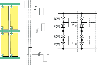
Fig. 4: Four subpixels in a shared select array layout with drive scheme and equivalent circuit.