A preview of the papers appearing in the May 2006 issue of the Journal of the SID. To obtain access to these articles on-line, please go to www.sid.org
Edited by Aris Silzars
Key design issues for autostereoscopic 2-D/3-D displays
Graham J. Woodgate
Jonathan Harrold
Ocuity, Ltd.
Abstract — Flat-panel 2-D/3-D autostereoscopic displays are now being commercialized in a variety of applications, each with its own particular requirements. The autostereoscopic display designer has two key considerations to address in order to meet customer needs – the optical output of the display (defined by the output window structure) and the choice of optical components. Window structure determines 3-D image resolution, achievable lateral and longitudinal viewing freedom, crosstalk, and 3-D fringe contrast. Optical-component selection determines the quality of the imaging of such windows, viewing distances, device ruggedness, thickness, and brightness. Trade-offs in window design are described, and a comparison of the leading optical component technologies is given. Selection of Polarisation Activated Microlenses™ architectures for LCD and OLED applications are described. The technology delivers significant advantages particularly for minimizing nominal viewing distances in high-pixel-density panels and optimizing device ruggedness while maintaining display brightness.
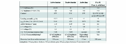
TABLE 3 — Comparison of reconfigurable 2-D/3-D optical-component technologies.
Tiling technology for large-area direct-view displays
A. C. Lowe
N. A. Gallen
P. A. Bayley
Abstract — In this paper, the optical and system characteristics of large-area displays based upon ITrans tiling technology are described. The characteristics of these displays are compared to those of other large-area display technologies.
Light guides are injection moulded in a high-index transparent colorless polycarbonate polymer. The input end has a dimension that is a multiple of the pixel pitch of the light valve, in this case a standard active-matrix LCD. The output end has a dimension such that the output face of the tile is larger than the LCD panel and its bezel. The input and output ends are substantially rectangular. Because the injection moulding process requires a draft angle on the two halves of the tool, they are actually irregular hexagons, with two internal angles at 178° and four at 91°. Between the input and output ends, the cross section of the image guide changes. This is to accommodate the mechanical requirements of packing and bending and to accommodate the optical requirements of a uniform output luminance characteristic at all points on the tile.
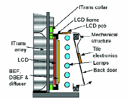
FIGURE 2 — Cross-section through an ITrans display.
The present and future of electronic paper
Alex Henzen
Jan van de Kamer
iRex Technologies
Abstract — With the rise of electrophoretic-display media from several sources, the world is opening up for new uses of electronic displays. Where "immersive reading" used to be a task strictly reserved for paper, displays can now fulfill that role. Many challenges still remain, such as full-color photograph-like performance and video speeds. However, in view of recent accomplishments showing near-video-speed switching and potential for full color, after electrophoretic displays obtain a slice of the reading market, application of these developments will take us a significant step towards full-color animated paper-like displays. The developments that have led to the presence of electronic paper in the market today will be described, and developments that are about to happen will be discussed.
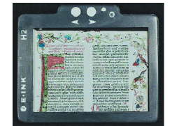
The true strength of electronic-paper technologies is their capability to position themselves in an application area that LCDs cannot reach: true paper-like readability at very low power. At the same time, developments are aimed at decreasing the difference between the response speed and color of LCDs. Extrapolating the improvements shown over the past 5 years gives an indication where the gap will be bridged. Color is slowly coming within reach. Iridigm/Qualcomm and Fujitsu are showing color displays, but electrophoretic displays combined with color filters show considerable promise, in the form of the color display demonstrated by E Ink (Fig. 3).
 (E Ink Corp.)
FIGURE 3 — Color prototype of an electrophoretic display.
A reflective-display QR-LPD®
Yoshitomo Masuda
Norio Nihei
Ryo Sakurai
Reiji Hattori
Bridgestone Corp.
Abstract — A novel reflective display [Quick-Response Liquid Powder Display (QR-LPD®)] has been developed. This paper-like display has the advantages of outstanding image stability, easy viewing, low-power consumption, and a high-response time. QR-LPD® will be promoted, initially, for use as electronic price-tag displays for merchandise. In addition, QR-LPD® is suitable for flexible-display applications because it does not require TFT arrays or a high-temperature process while maintaining an excellent paper-like image as well as glass-type display compatibility.
Figure 12 shows a seven-segmented display for clock use using the plastic-type QR-LPD® with a thickness of 0.29 mm and a weight of 7.7 g. The upper and lower substrates are composed of transparent plastic and FRP, respectively. The display can be bent up to a radius of about 20 mm. This segment display is driven by a static driving method, and voltage is applied through a contact hole in the rear substrate (FRP). This display shows a clear image since drawing electrodes are not present on the substrate surface. The two numbers on the left show the minutes, the middle ones show seconds, and the right ones show hundredths of seconds. The response time is less than 0.2 msec even for the plastic-type QR-LPD®. The dimensions of this panel are 5.5 cm in height and 10.5 cm in width.
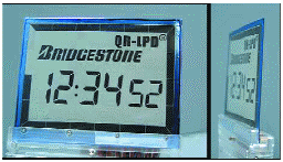
FIGURE 12 — Plastic-type QR-LPD® (segment).
Recent advances in phosphorescent OLEDs for small- and large-area-display sizes
M. S. Weaver
R. C. Kwong
V. A. Adamovich
M. Hack
J. J. Brown
Abstract — State-of-the-art phosphorescent organic light-emitting diode (PHOLED™) lifetime and efficiency performances for a range of emission colors are reported. Lifetimes in excess of 100,000 hours were demonstrated at display luminance levels for yellow-green and NTSC deep-red emission. In addition, external quantum efficiencies close to the theoretical maximum are demonstrated for long-lived PHOLEDs.
State-of-the-art PHOLED results are summarized in Table 1. Included in the table is a new sky-blue PHOLED recently reported with CIE coordinates (0.16, 0.37), a luminous efficiency of 22 cd/A (9.5% external quantum efficiency), and a half-life of 15,000 hours from an initial luminance of 200 cd/m2. Also included is a new green PHOLED with an efficiency of 65 cd/A at a display luminance of 1000 cd/m2 and a lifetime of 40,000 hours from this initial luminance. In this work, new materials and device architectures towards next-generation display requirements and ongoing work to maximize the efficiency-lifetime product of a full-color PHOLED system, and in turn to increase thecommercial prospects for OLED FPDs by using PHOLEDs, is reported.
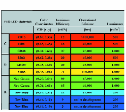
TABLE 1 — A summary of current commercial (C), development (D), and research (R) stage PHOLED performance.
Ink-jet printing: The route to production of full-color P-OLED displays
M. Bale, J. C. Carter
C. J. Creighton
H. J. Gregory
P. H. Lyon, P. Ng
L. Webb, A. Wehrum
Cambridge Display Technology
Abstract — Ink-jet-printing technology for displays has been making rapid progress and is now nearing production. This paper will go through the developments that have been carried out at CDT, Ltd., to achieve this status. The ink-jet head and machine development that underpin the capability of the RGB printing process to manufacture P-OLEDs at high speed with high reliability and with the film-forming properties to achieve the appropriate device performance will be described. The important contribution made by the availability of flexible metrological tools will be discussed.
There are, however, significant differences between the application of ink-jet printing for graphic arts and P-OLED displays. For printing P-OLED displays, it is necessary to achieve a high specification of both the drop placement and drop volume. The definition of reliability is also more stringent since, for displays, each drop counts and averaging techniques used to mask failing nozzles are not always possible to implement. In addition, the cost of the substrates is orders of magnitude higher than paper and card so that the cost of scrap is significant. Once the ink lands on the substrates, the processes that occur are also different. The display substrate is not porous, and significant development work has been undertaken to transform the printed droplet into films that achieve the electro-optical performance required for the display.
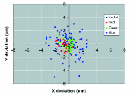
FIGURE 1 — Drop deviation from a range of nozzles of PEDT, red, green, and blue EL inks for a particular location on a substrate.
Video processing for active-matrix polymer-OLED TV
F. P. M. Budzelaar, C. N. Cordes,
J. J. L. Hoppenbrouwers
N. C. van der Vaart
W. H. M. van Beek, F. J. Vossen,
A. A. M. Hoevenaars
R. G. H. Boom
Philips Research Laboratories
Abstract — Active-matrix OLED panels have inherent features that allow a higher-quality image reproduction than LCD panels, i.e., high-contrast, fast response time, and the capability to produce locally high peak luminance levels. A 13-in. ink-jet-printed active-matrix polymer-OLED prototype for TV applications was demonstrated at SID 2004. This prototype is used as a carrier for studying video-processing algorithms that take full advantage of the specific characteristics of OLEDs. Addressing schemes, gamut conversion, histogram-based brightness control, and sparkle processing will be discussed.
OLED panels have extremely short response times. For LCDs, the LC material is responsible for poor long reaction times, causing motion blur. In contrast, for OLEDs it is the panel design and drive electronics that define the temporal behavior and is therefore much easier to modify. This freedom allows the circuit designers to combine desirable features into the panel. Key in the temporal behavior is the addressing scheme used. Addressing schemes with a low-duty-cycle value result in reduced motion blur. From a systems point of view, it is desirable to keep peak currents in the panel as low as possible to keep the voltage drop over the power lines, and thus unnecessary dissipation in the panel at an acceptable level. A suitable addressing scheme offers both.
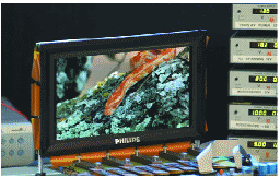
FIGURE 1 — Photograph of the 13-in. ink-jet-printed polymer-OLED prototype for TV applications.
Diffractive optics for virtual-reality displays
Tapani Levola
Nokia Research Center
Abstract — Near-to-eye (NTE) displays are generally systems where the imaging optics of a microdisplay is brought close to the eye, such as a magnifying glass. In portable NTE terminals, the challenges are in achieving low power consumption as well as low weight and small size. Part of the problem is related to the microdisplay, but the optics also plays a major role. A study on how diffractive optical elements (DOEs) on planar waveguides can be used to miniaturize the optics of NTE displays is presented and the performance of the system is analyzed.
The diffractive exit pupil expander (EPE) is geometrically accurate and achromatic, but it has severe problems in delivering uniform light distribution at the enlarged exit pupils. The uneven distribution is mainly due to the different path lengths of the light traveling inside the plate. This path length difference can be corrected using a stack of plates, which are separated from each other by low-refractive-index materials. The second major problem is the weak in-coupling of light into the plate. The angular dependence of the in-coupling can be minimized by a proper groove shape, but with the cost of efficiency. Exotic groove shapes might change this situation, but their feasibility in manufacturing remains to be seen.
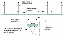
FIGURE 2 — Side view of an VRD having a diffractive EPE plate.
A method for reproducing apparent continuous depth in a stereoscopic display using "Depth-Fused 3D" technology
Hidenori Kuribayashi
Munekazu Date
Shiro Suyama
Toyohiko Hatada
Tokyo Polytechnic University
Abstract — A new method that can present fine depth increments in a stereoscopic display is proposed. In typical stereoscopic displays, depth can be presented by binocular disparity, but binocular disparity of less than one pixel cannot be displayed because, in general, electronic displays have discrete pixels. Binocular disparity and modulation of the edge luminance in DFD (depth-fused 3D) displays was combined. In an experiment, the perceived depth could be continuously changed by modulating the edge luminance only. Therefore, continuous depth can be produced by combining binocular disparity and modulation of edge luminance distribution.
In conventional stereoscopic displays, shapes of left- and right-eye images are identical, and the depth is perceived by binocular disparity. However, its depth resolution depends on the pixel pitch of the display for the left- and right-eye images. To overcome this problem, edges are placed in the luminance distributions, as shown in Fig. 2(c). Since these retinal images with mirror symmetry are the same as those in DFD displays, the subject would perceive continuous depth change, which is in proportion to the inner edge luminance.
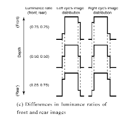
FIGURE 2(c) — Difference in luminance ratios of front and rear images. When the luminance ratios of both images were modulated, the left- and right-eye retinal luminance distributions changed.
Protective layer for high-efficiency PDPs driven at low voltage
Yasushi Motoyama
Toshiharu Kurauchi
NHK Science and TechnicalResearch Laboratories
Abstract — The sustain pulse voltage of a panel for 66-kPa Ne + Xe (5–30%) with an (SrCa)O protective layer is 20–40% lower than that with an MgO protective layer. The luminous efficiency of the panel with a Ne + Xe (30%) (SrCa)O protective layer is 1.5 times that of the conventional panel with a Ne + Xe (10%) MgO protective layer; the sustain pulse voltages of these panels are almost the same. The power loss caused by panel capacitance is proportional to the second power of the sustain pulse voltage. Using the (SrCa)O protective layer for Xe (5–30%), the power loss is reduced by 35–60% compared with the MgO protective layer. It follows that, using the (SrCa)O protective layer, the Xe content can be increased with little power loss, and high-efficiency PDPs can be achieved. As for MgO and CaO with Xe ions, electrons are probably ejected from only the defect states. On the other hand, as for the SrO with Xe ions, it is likely that electrons can be ejected from not only defect states but also the valance band. This seems to be the reason why the driving voltage is lower with the (SrCa)O protective layer than with the MgO protective layer.
The use of higher Xe content produces a large increase in discharge efficiency and has recently been established as an effective way to improve luminance efficiency. The problem is that the firing and sustain pulse voltages also increase significantly with higher Xe. Therefore, for PDPs with a conventional MgO protective layer, the Xe content is limited to about 10% for practical purposes. To overcome this drawback, a high-frequency drive has been introduced to suppress the increase in the sustain pulse voltage and raise the luminous efficiency of high-Xe-content PDPs. In this paper, (SrCa)O protective layers are used instead of the MgO protective layer to reduce the drive voltages of high-Xe-content PDPs and achieve high-efficiency PDPs.
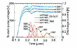
FIGURE 4 — Sustain pulse voltage and discharge current waveforms for 66 kPa Ne + Xe (5%) with (SrCa)O and MgO protective layers. Sustain pulses of 30 kHz were applied. Each discharge current waveform is the sum of current for 10 pairs of parallel electrodes.
Nano-emissive display technology for large-area HDTV
B. F. Coll
K. A. Dean
E. Howard
S. V. Johnson
M. R. Johnson
J. E. Jaskie
Motorola, Inc.
Abstract — Using nano-emissive display (NED) technology, Motorola labs has successfully developed 5-in. full-color display prototypes. Carbon-nanotube-based field-emission displays with a pixel size of 0.726 mm for a 42-in. HDTV exhibit video image quality comparable to CRT displays and demonstrate a luminance of 350 cd/m2. These novel low-drive-voltage NEDs take advantage of selective growth of CNTs to obtain the desired electron-emission performance while maintaining inexpensive manufacturing due to a simple self-focusing and self-regulating planar structure. Improved video image quality and color purity are achieved with very low power consumption and without the need for an expensive focusing grid.
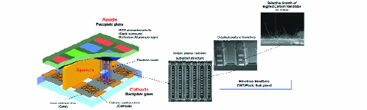
FIGURE 1 — Cut-away view of an NED structure (left) and emitter trenches, catalyst pads, and CNTs at increasing magnification (right).
Processes, characterizations, and system applications of color-filter liquid-crystal–on–silicon microdisplays
Ho-Chi Huang
Baolong Zhang
Huajun Peng
Hoi-Sing Kwok
Po-Wing Cheng
Yen-Chen Chen
The Hong Kong Universityof Science and Technology
Abstract — A color-filter liquid-crystal–on–silicon (CF-LCOS) microdisplay that integrates color filters on silicon for color will be presented. The color-filter process on silicon was optimized to achieve fine resolution and precise alignment of the color filters on the pixel array, good adhesion to the silicon suface, and a flat surface for the liquid-crystal cell assembly. Important optical and electrical parameters of the color filters were extracted to establish an electro-optical model of the CF-LCOS microdisplays for device simulation. Thermal, chemical, and light-stability characterizations were performed to ensure the stabilty of the color filters and CF-LCOS microdisplays. With color CF-LCOS microdisplays already available, the projection or viewing optics is greatly simplified. This CF-LCOS microdisplay is ideal for near-to-eye displays because of its low power consumption and compactness. The CF-LCOS microdisplay could also withstand medium light illumination for medium-sized projectors. A single-panel projector based on one CF-LCOS microdisplay of 1280 ´ 768 ´ RGB resolution was demonstrated.
The LCOS microdisplay is monochrome and requires a color technique to produce color. Conventional three-panel designs, which use three panels for three primary colors, are expensive. It is also very difficult to align three panels together with good accuracy in assembling optical engines. Another method that uses one panel and time-sequential color has made the optical system simpler. But it has to work with an electronic system of high data bandwidth and a liquid-crystal (LC) cell with fast response time. As a consequence, the system cost is high and the optical efficiency is low. Figure 1 illustrates a CF-LCOS microdisplay in which the color filters were coated directly onto silicon. The projection optics is greatly simplified because color is already available. What it needs is just a polarizing beam splitter (PBS) that directspolarized light into the display and back to a projection lens as also illustrated in Fig. 1.
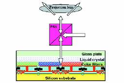
FIGURE 1 — Illustration of the CF-LCOS microdisplay.
Accurate determination of pretilt angle in twisted-nematic liquid-crystal cells by using a rotating analyzer
Michio Kitamura
Shunsuke Kobayashi
Katsumi Mori
Tokyo University of Science and Technology
Abstract — A new optical method for determining the pretilt angle Ψ, particularly on twisted-nematic (TN) liquid-crystal (LC) cells, is proposed. Ψ0 was rapidly determined with good reproducibility on a TN-LC cell by using a rotating analyzer optical system, a twist angle Φ, the azimuth of the director at a substrate, ψ0, and the retardation Δnd as known values. The thickness d was also determined simultaneously with Ψ0. Ψ0 and d within minutes. Ψ0 was previously determined to be in the range of 0.1° with a standard deviation of 0.01°; this was obtained by repeating the measurement 50 times. The principle behind the determination and the experimental set up are described in detail.
The measuring system is illustrated schematically in Fig. 5. The light source is a Xe short-arc discharge lamp. The light flux is focused on an entrance slit of a monochromator, which is in the Czerny–Turner configuration. The monochromatic light (the wavelength 633 nm is chosen) emerging from the exit slit is coupled to a multimode single cored optical fiber. A collimator attached to the other end of the fiber transmits a parallel light beam with a diameter of 4 mm. The spectral width is 2 nm at half-maximum. A Glan-Thompson prism generates the linear polarization.
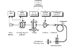
FIGURE 5 — Schematic diagram of the experimental setup.