OLEDs: The Challenges Ahead
Despite the widely acknowledged benefits of OLED-based displays, the technology has struggled to achieve market share, especially its active-matrix products. What hurdles remain to be conquered in order for OLEDs to achieve widespread acceptance?
by Amal Ghosh and Steven Van Slyke
IN the nearly 30 years since the observation of efficient organic thin-film electroluminescence by Ching Tang at Eastman Kodak Co., advances in stability and efficiency as well as the development of device structures with emission throughout the visible spectrum, have enabled organic light-emitting-diode (OLED) technology to be commercialized in both passive- and active-matrix display formats. Some of the key benefits derived with OLED-based displays include high-speed flicker-free video, wide viewing angle with high contrast, low power consumption, and excellent color gamut.
The total market revenue from OLED displays in 2005 was approximately $600 million. Although significant, this is still less than 1% of the overall flat-panel-display (FPD) market revenue of about $70 billion. OLED-based displays must address key technological challenges in order to gain market share and become a dominant FPD technology. To this end, the most important issues that face the OLED community will be discussed in this article.
A Brief History
In 1987, the first paper1 from Kodak describing efficient thin-film electroluminescence from a simple undoped structure was published. A follow-up paper2 in 1989 discussed the concept of doping the emission layer with various materials in order to modify the emission wavelength, as well as enhance the emission efficiency. These two papers created significant worldwide interest in OLED technology, both in industry and academia, because of the simple architecture, low drive voltage, and the relative ease of tailoring the emission properties by variations in the organic chemical structure. The first OLED display product, an aftermarket automobile traffic-information monitor, was introduced by Pioneer Electronics in 1996. This mono-chrome green display (256 x 64) was quickly followed by area-color passive-matrix OLED (PMOLED) displays with regions of blue, green, yellow, and orange emission. The PMOLED display market has continuously grown; today, monochrome and full-color displays are incorporated into cellular telephones (primarily in sub-displays), MP3 players, and other low-pixel-count applications. In fact, 20–25% of the displays in MP3 players produced in 2005 contain OLED displays. Kodak has broadly licensed the passive-matrix technology (now with about 20 licensees), and major PMOLED producers are located throughout Asia, the largest being Pioneer Electronics (Japan), Samsung SDI (Korea), and RiTDisplay (Taiwan).
 Eastman Kodak Co.
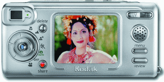
Fig. 1: Kodak's EasyShare LS633 digital still camera with an AMOLED display.
In 2001, Kodak and Sanyo Electric formed a joint-venture company, SK Display in Gifu, Japan, with the intent of fabricating full-color active-matrix (AMOLED) displays on low-temperature-polysilicon (LTPS) substrates. The first product containing a direct-view full-color AMOLED display, the Kodak EasyShare LS633 digital still camera, was introduced in 2003 (Fig. 1). The display was fabricated at SK Display by shadow masking the individual R, G, and B emitters.
In 2001, eMagin Corp. introduced a high-resolution (SVGA) full-color active-matrix top-emitting microdisplay fabricated on single-crystal silicon for near-to-eye applications (Fig. 2). The microdisplay format allows a user, effectively, to view a very large video screen from a tiny, portable source. This achievement was significant in that it demonstrated for the first time the use of a white top-emitting structure with color filters. The color filters were placed directly over the OLED structure – a process enabled by the development of a very robust thin-film seal over the transparent cathode. eMagin's OLED microdisplays represented the world's first AMOLED display, as well as the first OLED microdisplay to be commercialized.
In 2005, Sony commercialized a personal digital assistant (PDA), the Clie VZ-90, incorporating a 3.4-in.-diagonal full-color AMOLED display. As with the Kodak EasyShare LS633 camera, the display was fabricated on an LTPS backplane.
Although all these active-matrix display products are significant from a technological standpoint because they demonstrate the virtues of OLED technology – large viewing angle, low power consumption, excellent contrast ratio over all viewing angles, and high color gamut – revenues for AMOLED displays are relatively insignificant compared to those of PMOLED displays, mostly as a result of yield issues related to the active-matrix backplanes.
Aside from commercial OLED display products, technology demonstrations continue to show the virtue of OLED display performance. Each year, displays of larger sizes and higher quality are showcased and generally gather the largest crowds at tradeshows worldwide.
With passive- and active-matrix products introduced, plus impressive technology demonstrations, the question remains: What is holding back OLEDs from becoming a mainstream display technology? To answer this question, we first need to understand the critical challenges that face OLED technology.
Lifetime and Efficiency
Clearly, the display luminance half-lifetime required is application-dependent. For example, the lifetime requirement for a digital-camera display, which is generally used for displaying images, is much lower than the lifetime required by applications in which fixed icons or banners are frequently displayed, as in the case of notebook computers. A common lifetime target value used in the OLED community is "greater than 10,000 hours" from the initial luminance. This lifetime is usually assumed to be the time allowed for the display luminance to decay to one-half of the initial luminance. This may under-estimate or overestimate the actual lifetime required for the application.
As is to be expected, little information is available on OLED display lifetime in the literature, but a wealth of data on single-pixel test structures (usually in the 0.05–0.1-cm2 size range) exists. Also, much of the lifetime data provided on test devices is difficult to convey into usable product-life expectations. The single-pixel test-structure information is useful from a technology-comparison standpoint, but the extrapolation to display lifetime is far from straightforward as a result of the various factors that can affect display lifetime. For example, one of the more important factors that is generally not taken into consideration is the increase in operating temperature at the same luminance as the display size increases. It is also important to recognize that the luminance at the pixel level is much higher than the display luminance when the aperture ratio (the ratio of the emitting area to the non-emitting area within the display) is considered. This luminance difference can approach a factor of 10 for the individual R, G, and B subpixel colors and is highly dependent on the color coordinates of the R, G, and B primaries and target display color temperature.
OLED-emitting materials are available as both triplet and singlet emitters. Triplet emitters are typically higher efficiency (cd/A) compared to singlet emitters because triplet emitters have three (or four) excited states available for radiative relaxation to the ground state, compared to one for the singlet emitters. As the efficiency increases, the drive current density required for a particular luminance level decreases, an important factor for the lifetime as well as display power consumption. The typical operational stability levels (from 500 to 1000 cd/m2 initial luminance) reported for the triplet- and singlet-emitting formats are on the order of 20,000–100,000 hours for the green and red emitters,3 respectively, while the blue is on the order of 10,000–15,000 hours for the singlet and significantly lower for the triplet configurations. In fact, improving the blue-triplet stability at an acceptable CIE target point is highly challenging, and significant R&D activities continue in attempts to optimize the efficiency and operational stability while maintaining the required chromaticity.

 eMagin Corp.
Fig. 2: eMagin Corp.'s SVGA microdisplay.
More recently, singlet OLEDs with high-efficiency white emission have been demonstrated4 with efficiencies of 15 cd/A for a D65 white and operational stability of about 50,000 hours from 1000 cd/m2. White emission is highly attractive for manufacturing reasons, which will be discussed in a following section.
It is also clear that the drive voltage should be as low as possible in order to minimize display power consumption. Recent activities at Kodak and elsewhere have reduced the drive voltage from the typical 6–8 V (at the commonly quoted reference current density of 20 mA/cm2) to 2.5–3.0 V.5 In general, the lower drive voltage is achieved by incorporating highly conductive electron- and hole-transporting layers within the structure and improving charge-carrier injection efficiency from the electrodes.
In summary, the operational stability is being continuously improved, with exceptional stability being observed for the red-, green-, and white-emitting formats. Expected advances in the blue stability for the singlet and triplet emitters will soon expand the range of applications that will be accessible to OLED technology.
Color Patterning
There are essentially two techniques for producing full-color emission in OLED displays: those that require patterning of the OLED emitter and those that do not. These methods are shown in Fig. 3. Depositing the R, G, and B emitting layers in a pattern-wise fashion provides the best display power efficiency. However, the display color balance is difficult to maintain over time because the emitting materials are different for each color and degrade at different rates. The second method – depositing an unpatterned emitting layer and using a color-filter array or color-change medium to provide the R, G, and B emission – is attractive because there is no need to pattern the individual R, G, and B emitters. However, the power efficiency is compromised due to the absorption losses (color-filter approach) or absorption/re-emission losses (color-change process).
Pattern-wise deposition of the emitters is being used in manufacturing to fabricate full-color passive- and active-matrix displays. This method utilizes a thin metal shadow mask (stencil) to define the appropriate deposition regions on the substrate. Typically, the shadow mask is very thin (on the order of 10–20 μm) and is pulled against the substrate using a magnet. This process is repeated, with appropriate realignment, for each of the R, G, and B emitting layers. Unfortunately, this approach is costly (mask cost is high) and probably not scaleable beyond Gen 4 substrate sizes (730 x 920 mm), largely a result of the difficulty in controlling the thermal expansion of the mask caused by radiative heating from the evaporation sources. Although there is little published information available for this process, it is likely that repeated contact of a shadow mask with the substrate could also introduce defects.
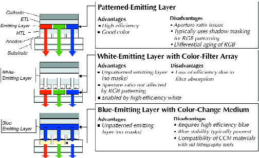
Fig. 3: The advantages and disadvantages of color-patterning methods for OLED displays. (Top) Patterened-emitting layer. (Middle) White-emitting layer with color-filter array. (Bottom) Blue-emitting layer with color-change medium.
An alternative to shadow masking is to deposit the individual colors using laser thermal processes, similar to thermal printing, where a donor sheet (blanket-coated with the appropriate emitting material) is placed adjacent to the substrate, and a laser is used to pattern-wise transfer the emitting material fromthe donor to the substrate. This is repeated three times with R, G, and B donor sheets and has been used to successfully demonstrate a 17-in. AMOLED through a joint effort between Samsung SDI and 3M in 2004. It is thought that the most critical problem facing this technology is the precise contact requirement of the substrate to the donor sheet, which must be uniform, without "tenting" (caused by particles, for example) that could prevent well-defined emission-layer deposition.
The non-shadow-mask approach using a white emitter with R, G, and B color filters formed on the substrate was demonstrated several years ago in a 15-in. format through a joint development effort between Sanyo and Kodak. Although this showed that an unpatterned emitter format is viable, the power consumption was too high for most practical direct-view display applications. A few years later, Kodak demonstrated an interesting approach to reducing this power consumption. This method incorporated a white-emitting subpixel in addition to the R, G, and B subpixels. The design has the advantage of reduced power – one-half the required power compared to the analogous white-based RGB display – and it is particularly well suited for imaging applications (digital cameras, TVs, portable DVD players, etc.). The reduction in power consumption results from the fact that there is very little saturated color content in typical images. Figure 4 shows the probability of a particular pixel color in a set of 13,000 digital still camera images. The high probability centered at the white point indicates that the world is "gray," i.e., images contain largely unsaturated color. This means that the white subpixel can be utilized frequently and, because it is not filtered, the display will consume relatively less power. This is clearly shown in Fig. 5. Any color in the sub-triangle that is defined by the R, G, and W primaries, for example, can be produced by the appropriate mix of these colors (no blue required). As the desired pixel color moves toward the W primary, proportionally more emission is provided by the highly efficient unfiltered W sub-pixel. Samsung Electronics recently implemented this technology in a 40-in. AMOLED display demonstration, the largest OLED display fabricated to date.
As a consequence of pixel size, the issue of color patterning for microdisplays is quite different from that of conventional direct-view displays. For example, a typical eMagin Corp. product has a subpixel pitch of 3.5–5.0 μm. At this size, the use of shadow masks to deposit the individual R, G, and B emission layers is extremely difficult. Consequently, the non-shadow-mask approach utilizing white emission with color filters was developed. Significant technology challenges were overcome for the single-crystal-silicon substrate configuration, which requires a top-emitting format, including developing the technology to place the color-filter array directly over the OLED layers. This required the development of a pinhole-free thin-film encapsulation in order to allow the color filters to be processed using conventional photolithographic techniques. This architecture also required new variations of high-efficiency long-life white OLED structures tuned to give the appropriate chromaticity when combined with the color filters.6
Backplane Issues
Arguably, the most difficult aspect of fabri-cating high-yield direct-view AMOLED displays is the presence of "muras" caused by TFT non-uniformities. These non-uniformities are caused by localized differences in TFT properties, which ultimately result in variations in current levels supplied to the individual subpixels throughout the display. From the visual standpoint, this results in areas of higher and lower emission, many times observed in a pattern representing a particular procedure used in the backplane-manufacturing process. For example, in the fabrication of LTPS backplanes, a laser anneal step is typically used for converting the deposited amorphous silicon (a-Si) to the higher mobility LTPS. "Horizontal streak mura" has been observed7 as a result of laser power non-uniformities, as shown in Fig. 6.
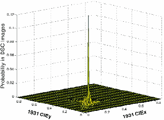
Fig. 4: Probability of pixel color determined by analysis of 13,000 digital still-camera images. Note the high probability of unsaturated color.
It is important to realize that the same backplane processes that provide high-quality active-matrix LCDs (AMLCDs) are often inadequate for OLEDs. This is based on the important distinction that the light emission in an OLED is controlled by the current level provided to the pixel, whereas the light emission from the LCD relies only on providing a voltage to the LC material. Slight variations in thin-film-transistor (TFT) processing can result in significant changes in the current delivered to the OLED pixel with the same input signal, causing non-uniformities. For LCDs, this is not as much of an issue because the drive voltage is quite uniform for a given gray-scale level.
There are many ongoing activities directed at eliminating muras, including improving the basic TFT-forming process and incorporating complicated compensation circuits within the pixel area. As with all the challenges for OLEDs, this technical area is know-how rich, and multiple solutions may exist for the same problem.
It was originally thought that only LTPS could provide the current levels necessary for AMOLED displays and, hence, the first demonstrations (and products) were fabricated on LTPS backplanes. With improvements in both OLED efficiency and a-Si mobility, however, a 20-in. AMOLED display was developed and shown in 2003 through a joint effort between Chi Mei Optoelectronics (CMO) and IBM. While it is difficult to judge whether a-Si exhibits as many mura issues, it is known that the short-range (pixel-to-pixel) uniformity of a-Si is significantly better than LTPS.
LTPS and a-Si backplanes are both being evaluated for AMOLED displays. LTPS will likely remain the technology of choice for small displays, where the high mobility enables integrated drivers on the display substrate, reducing module size. Whether a-Si is acceptable as an AMOLED backplane remains to be determined. Clearly, the instability associated with passing current through a-Si is an issue that confounds the overall display stability, but the large installed manufacturing base of a-Si backplanes and the fewer mask levels relative to LTPS makes this technology highly attractive. Consequently, significant worldwide activities are aimed at understanding, and solving, this instability.
For microdisplays, single-crystal silicon is used by eMagin Corp. as the backplane, which offers the ability to control the active-matrix array and also provides embedded high-speed controllers, clocks, and other graphics functions. Even here, great care must be taken in the integrated-circuit (IC) design to minimize the sub-threshold variations found in single-crystal-silicon complementary metal oxide semiconductor (CMOS) wafers.
Unit-Manufacturing Cost
One of the major benefits of OLED displays compared to LCDs is the perceived lower unit-manufacturing cost, which is easily understood when one considers that OLED displays do not require backlights and the associated light-management films. However, the installation base for AMLCDs is huge, with Gen 7 fabs in production and Gen 8 lines being constructed. One needs only to examine the price decline for LCD televisions to understand that the manufacturing cost for AMLCDs is being lowered rapidly as a result of this investment in capacity.
What is the status of OLED manufacturing? For PMOLEDs, capacity is being expanded both by existing manufacturers (RiTDisplay, Pioneer, Samsung SDI, and TDK) and newer players, such as Ness Display (Korea). It is expected that the market for PMOLED displays will continue to grow rapidly for displays with low row counts, both in monochrome and full-color formats. For AMOLEDs, almost all the major display manufacturers are investing in manufacturing facilities, and the focus is on full-color displays. For example,
• LG.Philips LCD has announced plans for a Gen 5.5 AMOLED fab.
• Chi Mei Electroluminescence Corp. (CMEL), a division of CMO, has installed a 620 x 375-mm OLED vapor deposition line and expects AMOLED production in 2006.
• Samsung SDI has announced plans to spend $465 million on a Gen 4 AMOLED manufacturing facility in 2006.
• Toppoly Optoelectronics plans to be in volume production in 2006, with the primary product being displays for small portable applications.
With an increase in capacity, it is expected that OLED-display manufacturing cost will fall, with the target, of course, being a lower cost relative to the analogous LCDs. Given enough time, this will happen. In fact, AMOLEDs are beginning to leverage existing AMLCD backplane facilities that are fully depreciated Gen 4 (and smaller) fabs, which will hasten the introduction of products containing AMOLED displays.
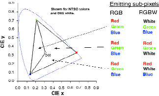
Fig. 5: Chromaticity diagrams showing the subpixels required for a particular color for RGB and RGBW displays. Note that for any color within the outer color triangle, two primaries plus the white subpixel can be used with the RGBW format.
For OLED microdisplays, eMagin Corp. continues to make progress in advancing the highest pixel-density OLED displays on silicon wafers. Higher-resolution and smaller- pixel-pitch AMOLED microdisplays are expected to be introduced in 2006. This is driven largely by cost: as SVGA displays become smaller, more displays can fit on a CMOS wafer with the cost per pixel being greatly reduced.
Conclusion
Certainly, there are challenges ahead for the OLED industry. There is little doubt, however, that PMOLED and AMOLED displays will continue to gain market share, at first limited to smaller displays used mostly in handheld applications and then expanding to the larger formats as the technical challenges addressed in this article are resolved. It is difficult to predict when OLED displays will begin to compete with LCDs in larger formats, such as the TV market. History has shown that scientific breakthroughs and important technology developments occur frequently in this field, which, along with the major investments in capacity and manufacturing tools by the foremost AMLCD manufacturers, will undoubtedly hasten that arrival.
In near-to-eye applications, the AMOLED-on-silicon approach is being incorporated into new applications ranging from 3-D video-game visors (Fig. 7) to portable media viewers for industrial and military use. This market is beginning to grow rapidly in part because of the unique viewing and low-power characteristics of the OLED.
References
1C. W. Tang and S. A. Van Slyke, Appl. Phys. Lett. 51, 913 (1987).
2C. W. Tang, S. A. Van Slyke, and C. H. Chen, J. Appl. Phys. 65, 3610 (1989).
3Note that these lifetimes are typically projected from a few thousand hours of operation.
4T. K. Hatwar, J. P. Spindler, and S. A. Van Slyke, Proc. EL (2004).
5J. Birnstock, M. Hofmann, S. Murano, M. Vehsi, J. Blochwitz-Nimoth, Q. Huang, G. He, M. Pfeiffer, and K. Leo, SID Symposium Digest Tech Papers 34, 40 (2005).
6A. P. Ghosh, Proc. SPIE 46th Intl. Symp. Optical Science and Technology (2001).
7J. W. Hamer, A. Yamamoto, G. Rajeswaran, and S. A. Van Slyke, SID Symposium Digest Tech Papers 34, 1902 (2005). •
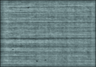
Fig. 6: Contrast-enhanced image of an emitting AMOLED display (on LTPS) showing horizontal streaks due to variations in the laser annealing process.
 eMagin Corp.
Fig. 7: eMagin Corp.'s 3-D video-game visor.
Amal Ghosh is Vice President, Display R&D, for eMagin Corp., 2070 Route 52, Hopewell Junction, NY 12533; telephone (845) 838-7918, e-mail: aghosh@eMagincorp.com. Steven Van Slyke is Research Fellow and Director, Display Technology Unit, OLED Systems SPG, Research Laboratories, Eastman Kodak Co., Rochester, NY 14650; telephone (585) 722-1222, e-mail: steven.vanslyke@kodak.com.
Please login above to view the entire article