Manufacturing Equipment and Methods Seen at SID 2006
Because of the increasing importance of yield and testing along with the growing sizes of display panels, manufacturing equipment and methods were areas of acute interest at SID 2006. Here are some of the highlights.
by Peter Smith
AS THE RACE for ever-bigger display panels continues, with billions of dollars being invested in new fabs that can support glass sizes of Gen 7 and larger, the technology that drives display manufacturing has become more critical than ever. Because of growing display sizes, the emphasis on yield and test is increasing. As a result, new methods in test and metrology are coming online, and many innovations in front-end device-fabrication equipment technology were demonstrated at SID 2006 held in San Francisco. These breakthroughs typically combined new materials and processes, resulting in lower cost of ownership and functionality previously unattainable. Innovations in panel assembly were aimed at improving back-end yield while permitting increasingly narrow pitches required by high-information-content mobile displays. Here is a look at some of the specific developments.
Device Fabrication
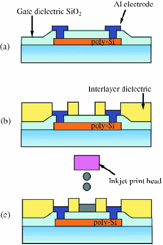
Xaar, imaging Technology international (iTi), and Cima NanoTech released a turnkey solution for silver nanoparticle printing for flat-panel-display fabrication [Fig. 1(a)]. The solution combines Xaar's innovative OmniDot piezoelectric ink-jet technology [Fig. 1(b)] with iTi's fabrication tool for digital printing [Fig. 1(c)] and Cima Nanotech's silver ink. The targeted applications include printed transistor technology as well as plasma-display panels (PDPs). For printed transistor technology, the use of the approach could enable the electrode layers to be formed with low cost of ownership. For PDP electrodes, the challenge is to replace the copper mesh currently employed for EMI shielding.
Peter Smith is with Honeywell, 101 Columbia Rd., CTC 3-003, Morristown, NJ 07960-4640; telephone 201/454-1786, fax 973/455-3458, e-mail: peter.smith@honeywell.com.
Fig. 1: Xaar, imaging Technology international (iTi), and Cima NanoTech have released a turnkey solution for silver nanoparticle printing for flat-panel-display fabrication (a). The solution combines Xaar's innovative OmniDot piezoelectric ink-jet technology [printhead, (b)] with iTi's fabrication tool for digital printing (c) and Cima NanoTech's silver ink.
Cabot Corp. gave an update on the progress of its silver-ink technology (paper 65.4, Vanheusden, et al.). Seiko-Epson Corp.presented a paper on how Ulvac's silver ink could be used in the fabrication of low-temperature-polysilicon (LTPS) devices (paper 48.1, Shioya, et. al.), as shown in Fig. 2. The current approaches for silver ink are focused on replacing bus lines. As printing technology advances with respect to transistor fabrication, the need to route signals in and out of the device cannot be overlooked.
By further employing the ink-jet process, Seiko-Epson claimed use of the technology in a mass-production process to form an alignment layer on high-temperature-polysilicon (HTPS) TFT liquid-crystal panels used in LCD projectors.
The University of Cologne and Merck KGaA demonstrated an alternative to ink-jet technology called direct photolithography for OLED manufacturing (poster paper 181, Prof. K. Meerholz). Most processing steps are solution-based; the entire fabrication process is simple and cost effective. Spin-coating is used to deposit each polymer onto a transparent substrate. The polymer film is then irradiated with ultraviolet light through a shadow mask, causing the polymer to cross-link and to form an insoluble material. The non-cross-linked material in the non-illuminated areas of the film is then washed away with solvent. The two other polymers are subsequently deposited in the same way to fabricate the pixelated device with three individually addressable colors.
The direct-lithography technique can easily achieve high resolution and does not struggle with film-thickness variations. A super-high resolution of 2 μm (equivalent to much more than 1000 ppi) was demonstrated on standard commercial and untreated display motherglass. Even more importantly, there is no need to separate the pixels by the use of special ink-confinement structures. Direct photolithography allows for extremely small pixel spacings and high fill factors. As a consequence, the current density during display operation can be decreased, which reduces the power consumption and has a positive effect on the device lifetime.
 Seiko-Epson
Fig. 2: Seiko-Epson's schematic illustration of their TFT fabrication process for making the top-gate contact of an LTPS TFT for LCDs and/or OLEDs.
Assembly Process and Equipment
Pixel Interconnect, Toddco, and Ohashi Engineering (which exhibited at the Ito America booth) showed equipment and processes aimed at completing display-panel assembly. Critical to achieving this back-end capability is Sony Chemical's anisotropic conductive film (ACF). Sony Chemical showed ACF with shorter process times (5 sec for bonding) and particles that permit finer interconnects down to 12 μm. These innovations are critical to high-resolution small-form-factor displays.
Test
As glass-panel size increases to serve the LCD-TV market and capital investment skyrockets, the need to achieve higher yield in a shorter time is ever-present. Orbotech presented its latest approach in aiding display manufacturers in their efforts to achieve this goal (paper 59.3, Adin, et al.). Orbotech's approach is to emphasize automatic defect classification for assessment of glass substrates. Orbotech emphasized the combination of image-analysis algorithms that included learn- and rule-based computations. This permits the display manufacturer to tailor the test routine to their specific, emerging, and changing requirements.
Metrology
Dai Nippon Screen Manufacturing Co. presented a method to detect mura on a coated photoresist layer in the manufacturing line of display devices (paper 59.1, Ueta, et al.). Why is this important? The presence of mura – defined as irregular non-uniformity of transmittance or reflectance on a surface – in coatings used in display fabrication results in yield loss. Typically, mura are inspected by tilting the glass panel, but with glass dimensions now exceeding 2 m on the diagonal, this is no longer a good idea.
Rather than tilting the glass, Dai Nippon illuminates the glass via a set of narrow-band-pass-filtered light of different wavelengths. The intensity of the reflected light from the film is a periodical function of the layer thickness by the interference of the surface and bottom reflection of the layer; therefore, detection sensitivity of the mura, which is a local variation of the thickness, changes. The apparatus is enabled to detect the thickness variation of several nanometers. •
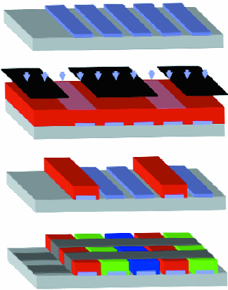
Fig. 3: Schematic illustration of the direct photolithography process for the fabrication of a full-color OLED display demonstrated by the University of Cologne and Merck KGaA at SID 2006. The red-emitting polymer is spin-coated onto the substrate with an ITO comb structure and selectively exposed to UV light using a contact mask aligner. Subsequently, the non-cross-linked parts are dissolved, and the procedure is repeated for the green and the blue emitters. Finally, cathode rows are deposited by thermal evaporation through a shadow mask.