A preview of the papers appearing in the September 2005 issue of theJournal of the SID, available on-line at www.SID.org.
Edited by Aris Silzars
Carbon-nanotube electron emitters for display applications
Ajita Patil
Linchung Li
Liming Dai
Michael Casavant
Karla Strong
University of Dayton
Abstract — The optoelectronic, mechanical, and thermal properties of carbon nanotubes have made them very attractive for a wide range of potential applications. However, many applications require the growth of aligned/micropatterned carbon nanotubes with or without a modified nanotube surface. Several simple pyrolytic methods for large-scale production of aligned carbon-nanotube arraysperpendicular to the substrate surface have been developed. Photolithographic and soft-lithographic techniques have also been used to pattern the aligned carbon nanotubes with submicron resolution. These aligned carbon-nanotube arrays can be transferred onto various substrates of particular interest (e.g., on conducting substrates as electron emitters for flat-panel displays) in either a patterned or non-patterned fashion. The well-aligned structure further allows for the preparation of aligned coaxial nanowires of carbon nanotubes sheathed with polymers and to modify the surface of individual carbon nano-tubes by plasma treatment. These aligned/micropatterned carbon nanotubes with and without surface modification possess desirable properties for electron emission applications.
To construct aligned CNT arrays on conducting electrodes for electron-emitting measurements, a thin layer of gold was sputter coated onto an as-synthesized aligned nanotube film. The gold-covered CNT film was then separated from the quartz glass plate used for the nanotube growth with an aqueous solution of 30% HF. The electron-emitting property of the aligned carbon-nanotube array was then measured using gold foil as a conducting substrate.
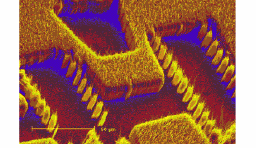
FIGURE 2 — Typical SEM micrographs of patterned films of aligned nano-tubes prepared by the pyrolysis of FePc onto a photolithographically pre-patterned quartz substrate.
Fabrication of CNT field-emitter array using a polymer insulator
K. Nishimura
N. Yasuda
T. Shiroishi
A. Hosono
S. Nakata
S. Okuda
Mitsubishi Electric Corp.
Abstract — The fabrication process of a carbon-nanotube (CNT) field-emitter array (FEA) having a polymer insulator is reported. This polymer material is suitable for a large-sized FEA because of its coating property and thermal stability. These features contribute to the display-image uniformity, the tolerance to the thermal-sealing process,
etc. A new method of forming via holes on the insulator instead of gate holes has been developed. The method uses a spin-wet-etching (SWE) technique instead of the typical reactive-ion-etching (RIE) method. The RIE method damages and contaminates the CNT at the end of the etching process. However, the SWE technique ensures fine gate hole configurations with little under-cut without any damage nor contamination. An FEA panel 1.5 in. on the diagonal was fabricated by using the method. The FEA showed good emission uniformity with proper surface treatment of the CNT.
The three samples were prepared as follows: (1) as-fired, (2) the PPSQ film on the CNT was removed by using a spin-wet-etching method, (3) the PPSQ film on the CNT was removed by using a RIE method. Laser irradiation was applied to each CNT before they were placed in the vacuum chamber. Figure 9 shows that the CNT of the spin-wet-etching method gained efficient emission current comparable to that of as-fired. While, on the other hand, the CNT of the RIE method showed little emission.
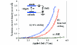
FIGURE 9 — The degradation of emission characteristics by using the spin-wet-etching and RIE methods. The inset shows the measurement system for the diode mode.
Uniform carbon-nanotube emitter for field-emission displays
Hiroyuki Kurachi, Sashiro Uemura,
Jyunko Yotani, Takeshi Nagasako,
Hiromu Yamada, Tomotaka Ezaki,
Tsuyoshi Maesoba, Takehiro Nakao,
Masaaki Ito, Akira Sakurai,
Yahachi Saito, Hisanori Shinohara
Noritake Co., Ltd.
Abstract — The synthesis of carbon-nanotube (CNT) field emitters for FEDs by thermal chemical vapor deposition (CVD) and their structural and emission characterization are described. Multi-walled nanotubes (MWNTs) were grown on patterned metal-base electrodes by thermal CVD, and the grown CNTs formed a network structured layer covering the surfaces of the metal electrode uniformly, which realized uniform distribution of electron emission. A technique for growing narrow MWNTs was also developed in order to reduce the driving voltage. The diameter of MWNT depends on the growth temperature, and it has changed from 40 nm at the low temperature (675°C) to 10–15 nm at the high temperature (900–1000°C). Moreover, narrower MWNTs were grown by using the metal-base electrode covered with a thin alumina layer and a metal catalyst layer. Double-walled nanotubes (DWNTs) were also observed among narrow MWNTs. The emission from the narrow CNTs showed a low turn-on electric field of 1.5 V/μm at the as-grown layer.
(a) (b)
FIGURE 2 — CNT layer deposited on a metal electrode. (a) Section of patterned CNT emitter. (b) Surface morphology of CNT layer.
FIGURE 8 — Emission distribution profiles (0–1 mA/cm2) of theCNTs grown by using the metal-base electrode covered with a thin alumina layer and a metal catalyst layer.
Pen-writable nanocarbon arrays fabricated using liquid-crystalline materials for potential use in displays
Matthew E. Sousa, Christopher Chan,
Yuming Gao, Sylvain Cloutier,
Kengqing Q Jian, Bevan S. Weisswan,
Gregory P. Crawford, Robert Hurt,
Nancy Yang
Brown University
Abstract — Carbon nanotubes and nanofibers using liquid-crystalline materials have been fabricated. By using these materials, the orientation of graphene layers can be manipulated using surface-anchoring techniques common to liquid-crystal displays. The bulk material properties of the graphene can be controlled by the spatial arrangement of the layers due to their anisotropic nature. A method to pattern arrays of these nanoforms using an automated printing technique has also been demonstrated.
Using the technique described, linear arrays of nanotubes 160 μm wide and 50 mm long were successfully fabricated. The length was only limited by the size of the alumina templates used during the printing process. SEM images of the resulting tubes can be seen in Fig. 4. In order to minimize the amount charging in the SEM, the samples were sputter coated with a thin layer of gold. The SEM images reveal that the tubes are mostly hollow, but have some internal membranes that separate the hollow interior into a series of cellular cavities. Reducing the concentration of indanthrone disulfonate in the system can eliminate these structures.
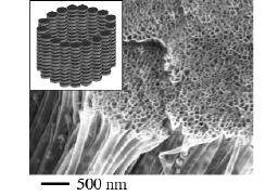
FIGURE 4 — An SEM image of the carbon nanotubes produced using the lyotropic liquid-crystalline carbon precursor. The inset is a schematic representation of the molecular structure of the nanotubes. The graphene layers are oriented such that they are orthogonal to the long axis of the nano-tube.
Effects of carbon-nanotube doping on the performance of a TN-LCD
Wei Lee
Yu-Cheng Shih
Chung Yuan Christian University
Abstract — The electro-optical characteristics of a 90° twisted-nematic liquid-crystal display (TN-LCD) were analyzed. The test cell was composed of a minute amount of dopant, multiwalled carbon nanotubes, and a standard nematic mixture, E7, used in TN-LCDs with direct addressing. Under the experimental conditions, no hystereses in optical transmittance were observed in either the doped cell or a neat counterpart under an applied ac voltage. Experimental results show that doping with nanotubes rectifies the electro-optical properties of the cells by reducing the driving voltage as well as the rise time. Similar results were found in a TN cell of a TFT-grade liquid crystal instead of the mixture consisting completely of polar compounds.
Figure 2 shows the frequency-dependent transmittances from 1 to 150 kHz for a fixed operation voltage of 3.0 Vrms. It is clear from Fig. 2 that the curves fall and rise monotonically for NB and NW modes, respectively, in the frequency range from 80 to 150 kHz. Not shown in the figure, similar measurements with a switching voltage of 4.0 Vrms yielded contrast curves all nearly constant between 1 and 150 kHz because the voltage 4.0 Vrms is far beyond the required driving voltages.
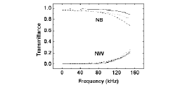
FIGURE 2 — Optical transmittance as a function of the frequency of an applied ac voltage of 3.0 Vrms in the ranges of 1–150 kHz for various TN cells. Dotted line, pure E7; solid line, CNT-doped E7; dashed line, C60-doped E7.
New non-synthetic method to modify properties of liquid crystals using micro- and nano-particles
O. Buchnev
C. I. Cheon
A. Glushchenko
Yu. Reznikov
J. L. West
Institute of Physics
Abstract — The modification of the properties of existing LCs by doping them with ferroelectric micro-and nano-particles will be reported. This approach, in contrast to the conventional time-consuming and expensive chemical synthetic methods, enriches and enhances the electro-optical performance of many liquid-crystal materials. The effect of the ferroelectric particles on the nematic, smectic, and cholesteric phases will be discussed. The performance of these new composite systems in various devices, including displays, light modulators, and beam-steering devices, will be reported.
Scattering in 16-μm-thick cells was produced by heating the cell above the clearing temperature and cooling it into the smectic phase. Applica-tion of an electric field orients the liquid crystal in a homeotropic state and the scattering disappears. Figure 5 shows the dependence of the intensity of the light passing through such a cell as a function of applied voltage. The threshold voltage for a cell filled with the pure 8CB LC was »10 V higher then the corresponding voltage for a cell filled with a mixture of 8CB and Sn2P2S6particles when their concentration was 0.36 wt.%. These experiments suggest that ferroelectric particles can improve the performance of many smectic LC devices, including bistable SmA displays.
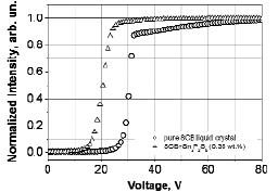
FIGURE 5 — Comparison of the electro-optic response of the cells filled with pure SmA 8CB LC and a mixture of the 8CB with Sn2P2S6 ferroelectric particles. The graph shows the transition from chaotical orientation of the LC in the cells to its defect-less homeotropic orientation.
Photostable liquid-crystal guest-host nano-materials for display applications
Nabil M. Lawandy
Andriy Y. Smuk
Nanosciences Corp.
Abstract — The optical plasmon absorption of anisotropic metallic nanoparticles in a liquid-crystal host medium was theoretically modeled. Metallic nanorods and spheroids act as pleochroic dopants with virtually unlimited photostability. Calculations predict that full-color displays based on nanorod orientation driven by the transition from homogeneous to homeotropic LC alignment are feasible. These displays are expected to have large viewing angles without the need for polarizers or LC anchoring surfaces.
Plasmon absorption from anisotropic metal nanoparticles and structures based on Au, Ag, Al, and other metals in LCs can be used to create completely photostable guest-host display materials. The color-switching effects in these novel systems occur due to the orientation of these metal nanostructures when the LC host undergoes a transition from the homogeneous to the homeotropic phase by the application of an electric field. The predicted display behavior may allow for large viewing cones and display structures which do not require anchoring surfaces and polarizers. Based on models, these new nanostructure-based materials and the displays developed around them may compete with the most advanced Super-IPS displays on the market today, but with greatly reduced fabrication costs and enhanced manufacturing yields.
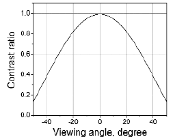
FIGURE 2 —Contrast ratio of the pixel as a function of the viewing angle.
Properties and characterization of carbon-nanotube-based transparent conductive coating
C. M. Trottier
P. Glatkowski
P. Wallis
J. Luo
Eikos, Inc.
Abstract — Transparent and electrically conductive coatings and films have a variety of fast-growing applications ranging from window glass to flat-panel displays. These mainly include semiconductive metal oxides such as indium tin oxide (ITO) and polymers such as poly(3,4-ethylenedioxythiophene) doped and stabilized with poly(styrenesulfonate) (PEDOT/PSS). In this paper, alternatives to ITO and conducting polymers, using single-wall carbon nanotubes (SWNT), will be discussed. These CNT-based technologies offer conducting substrates having a broad range of conductivity, excellent transparency, neutral color tone, good adhesion, abrasion resistance, and flexibility. Additional benefits include ease of both processing and patterning. This paper reports on optoelectronic properties and structure characterization of these materials.
The visible-light transmittance of ITO, PEDOT, and CNT films is shown in Fig. 4. The CNT film displays high transparency across the complete visible-light spectrum. In comparison, ITO has a maximum transparency in the range of 500–550 nm, at the expense of significantly lower transparency at other wavelengths. For the same level of conductivity, current CNT films show somewhat lower transparency at 550 nm compared to the peak transmittance of ITO. However, CNT films exhibit significantly higher transparency across the entire visible-light spectrum. CNT films are also much more transparent than PEDOT. The performance gap between CNT and ITO will be minimized by further product optimization.
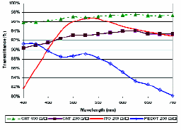
FIGURE 4 — Optical Performance. Visible-light transmittance of ITO, PEDOT, and CNT films.
Optics of sheared liquid-crystal polarizer based on aqueous dispersion of dichroic-dye nano-aggregates
M. Paukshto
G. Fuller
A. Michailov
S. Remizov
Stanford University
Abstract — The initial results on the optical properties of lyotropic liquid crystals under shear and following the cessation of flow are presented in the paper. Disk-shaped aromatic molecules that self-assemble into columnar nano-stacks in the water form the supramolecule – the basic structural element of these liquid crystals. The nature of the flow is an important factor determining the material microstructure, providing a global order and initial conditions for the drying process. The dried coating exhibits the properties of an E-type broadband polarizer. Understanding the dynamics of texture evolution and its interaction with the flow is of crucial importance to any development of polarizers coated with the liquid crystals.
The overall goal of this study is to improve the optical anisotropy of the Optiva N015 coatings, and initial results on the optical properties of thin layers under shear and following the cessation of flow are presented. The nature of the flow is an important factor in determining the material microstructure and understanding the dynamics of texture evolution, and its interaction with the flow is of crucial importance to any future development of polarizers coated with N015 liquid-crystal solutions.

FIGURE 11 — Schematic diagram of the shearing system attached to an Axometrics polarimeter.
Hybrid nano-coatings in the display industry
Edwin P. K. Currie
Mark Tilley
DSM Research
Abstract — In the display industry, there is an increasing use of polymeric coatings comprising inorganic nanoparticles. These particles endow the coatings optical, electrical, or mechanical properties not attainable with organic materials, while the use of an organic binder allows easy processing via,
e.g., wet deposition and UV or thermal crosslinking. Nanoparticles are relatively new materials and seem to offer numerous opportunities for new coatings for the display industry. Examples of this are silica nanoparticles in anti-reflection coatings, indium-tin-oxide particles in antistatic coatings, and metallic carbon nanotubes in conductive coatings. Yet the physical interactions that determine the dispersion of nanoparticles in the wet formulation and the resulting morphology in the dry coating can be traced back to classical colloid science. In this paper, some of these principles and their application to nanoparticles dispersed in organic solvents are focused upon. These principles will be illustrated with several examples of anti-reflection coatings, anti-static coatings, and hardcoats currently in use in the industry.
TABLE 1 — Overview of the most-common inorganic nanoparticles.
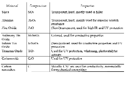
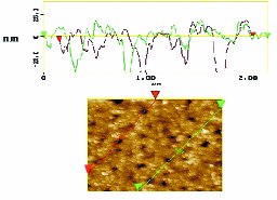
FIGURE 6 — AFM image of a nanocorrugated AR coating.
Tailored elliptical holographic diffusers for LCD applications
Jun Qi
Joel Petersen
Chris Rich
Wavefront Technology, Inc.
Abstract — In this paper, an LCD backlight with holographic diffusers as the top diffuser was investigated. Using a suitable elliptical holographic diffuser, the moiré pattern was eliminated and the brightness of the backlight was increased up to 15% compared to that for a backlight with a conventional diffuser. Monte Carlo simulation was also applied to compare with the experimental results. In addition, elliptical diffusers can be applied to modify the viewing cone of the backlight.
The principle of moiré pattern elimination using top diffusers is schematically illustrated in Fig. 8. The light after the reversed prismatic film carries the periodic information of micro-prisms. The addition of a circular top diffuser with suitable haze can mix the light and smear the periodic information to avoid the moiré pattern, as shown in Fig. 8(a). An elliptical diffuser with a lower full-width at half maximum (FWHM) on the minor axis can achieve the similar mixing power by increasing the FWHM on the major axis [see Fig. 8(b)]. However, there is a critical value for FWHM on the minor axis to attain the mixing effect. In the backlight, the critical FWHM is approximately 4–5°. This critical value is expected to be related to the pixel size of the LCD panel, so the optimal top diffuser may vary.
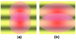
FIGURE 8 —Schematic illustrations of the principle of eliminating moiré pattern using a (a) circular and (b) elliptical top diffuser.
Viewing-angle enhancement in holographic reflective displays by nanoscale holographic patterning
Michael L. Ermold
Adam K. Fontecchio
Drexel University
Abstract — This work presents a method to increase the viewing angle of holographic polymer-dispersed liquid-crystal (H-PDLC) reflective displays. One of the drawbacks to H-PDLC technology is the existence of a narrow viewing angle. A way to alleviate this problem by structuring the phase front of the recording beams to increase the viewing cone of the display is presented. Analysis of the diffractive properties of these holograms shows that the macroscopic and the nanoscale morphologies both play a role in the optical properties of the films.
The technique used here made use of the interference of a diverging or converging spherical wave and a plane wave, shown in Fig. 1. A holographic optical element (HOE) that demonstrates ~100-nm-thick curved layers of polymer and liquid crystal is created through interference patterning. Specifically, a holographic parabolic mirror is formed with the ability to focus and/or to diverge the incident light. When illuminated from the same side as the spherical wave source, a focusing effect is observed in the HOE, where the source is reconstructed by the reflected light. The focal length of the holographic mirror is determined by the point-source–to–H-PDLC distance during the recording process, and in the experiments is on the order of 1–5 cm.
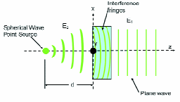
FIGURE 1 — Schematic showing the interference of a spherical wave with a plane wave.
Probing the supra-nano-scale and micron-scale structure of liquid-crystal and polymer dispersions using laser light scattering
Garfield T. Warren
J. B. Whitehead, Jr.
University of Southern Mississippi
Abstract — Liquid-crystal and polymer dispersions are typically made utilizing one of three methods of phase separation. Laser light scattering is a convenient method to probe the evolving supra-nano-scale and micron-scale morphology of phase-separating mixtures. We used laser light scattering to probe the evolving supra-nano-scale and micron-scale structure of phase-separating liquid crystal and monomer mixtures induced with photon-initiated polymerization. The evolutionary phase separation for mixtures of the E7 and the thiolene based optical adhesive Norland 65 from low to high weight percentages of E7 are reported.
LCPDs have potential application in the display, communication, and optical industries. The applications include reflective display technology, Bragg gratings, beam steering, reflective and transmission filters, optical interconnects, high-intensity laser radiation attenuators, etc. Liquid-crystal and polymer dispersions also provide an opportunity to investigate fundamental aspects of the phase separation of low-molecular-weight liquid-crystal and monomer mixtures prior to, during, and after polymerization. An in-depth understanding of the fundamental relationships between the materials, processing conditions, and micro-structural evolution is critical to the design and advancement of LCPDs to meet the requirements for application in the display, communications, and optical industries.
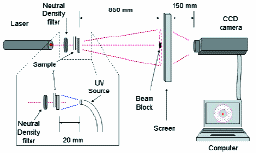
FIGURE 4 — Schematic of the experimental apparatus used to investigate the evolving phase-separated morphology of PDLC samples. Each sample was located 850 mm in front of the translucent screen while the CCD camera was 150 mm behind translucent screen. Illustrated in inset is the positioning of the UV light source.
Deformed nanostructure of photo-induced biaxial cholesteric films and their application in VA-mode LCDs
Ichiro Amimori
Satomi Suzuki
Fumio Obata
Christian Ruslim
Fuji Photo Film Co., Ltd.
Abstract — Novel biaxial retardation films made from photo-induced deformed cholesteric liquid-crystal (LC) nanostructures using reactive mesogen mixtures (RMMs) for a viewing-angle compensation of vertically aligned liquid-crystal displays (VA-LCDs) was developed. The deformed cholesteric LC nanostructure has been observed by X-ray-diffraction (XRD) measurement. The birefringence of the film was described well by an optical model based on a form birefringence theory. The VA-LCDs with photo-induced biaxial cholesteric films have excellent viewing-angle properties.
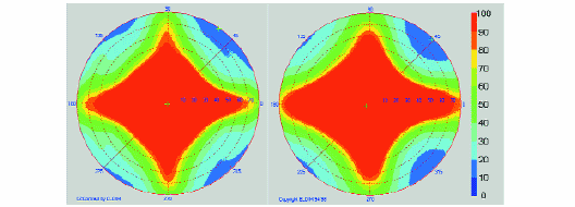
FIGURE 10 — Isocontour maps of (a) a compensated and (b) a commercial-product VA-LCD.
Photostability of liquid crystals and alignment layers
Chien-Hui Wen
Sebastian Gauza
Shin-Tson Wu
University of Central Florida
Abstract — Photostability of liquid-crystal (LC) materials and surface alignment layers were evaluated using a UV lamp and a blue laser beam. Both organic polyimide (PI) and inorganic silicon-dioxide (SiO2) alignment layers were studied under a nitrogen environment. Two commercial TFT-grade LC mixtures (low-birefringence MLC-9200-000 and high-birefringence TL-216) were used for comparisons. Results indicate that SiO2 alignment layers are much more robust than PI layers, and low birefringence LCs are more stable than the high-birefringence ones. At the He-Cd laser wavelength (λ = 442 nm), both LC mixtures and SiO2 alignment layers are hardly damaged. To lengthen the lifetime of an LCD projector, inorganic SiO2 alignment layers, high-optical-density UV filters, long-cutoff-wavelength blue filters, and short-conjugation (low birefringence) LC materials should be considered.
Photostability of liquid-crystal (LC) materials and alignment layers play a crucial role in affecting the lifetime of liquid-crystal-display (LCD) devices. In direct-view displays, ultraviolet (UV) light is often used to seal the LC panels. In projection displays using liquid-crystal–on–silicon (LCOS), the employed arc lamp is relatively bright. Although a cold mirror and a hot mirror are used to filter out the unwanted UV and infrared contents of the lamp, residual UV light could still penetrate into the LC panels and cause performance degradation. Even if the UV contents are completely filtered out, the blue wavelength might still be harmful to the LCD panels. These high-energy photons could cause gradual degradation of the organic alignment layers and the LC molecules. Once the LC medium is decomposed or the alignment layers deteriorated, the pretilt angle is changed and the consequent electro-optic effects are altered.
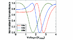
FIGURE 6 —The voltage-dependent transmittance of a PI-B alignment cell with MLC-9200-000 before (red line) and after (blue line) UV exposure. The UV intensity is 350 mW/cm2.