A preview of the papers appearing in the October 2005 issue of the Journal of the SID, available on-line at www.SID.org.
Edited by Aris Silzars
Effects of trace nickel on the growth kinetics and the electrical characteristics of metal-induced laterally crystallized polycrystalline silicon and devices
Dongli Zhang
Man Wong
Hong Kong University of Science and Technology
Abstract — An increase in the rate of nickel-based metal-induced lateral crystallization (MILC) of amorphous-silicon (a-Si) was observed when the length of an a-Si island was decreased or, for a given island length, when an extra crystallization-inducing window was added. With phosphorus implanted in a localized region offset from the MILC front on the a-Si side, a slight reduction in the MILC rate was also observed. Nickel incorporated in a-Si beyond the MILC front is believed to be responsible for these effects. A diffusion coefficient of ~4 ´ 10–8 cm2/sec was estimated for nickel in a-Si at 600°C. An extended low-temperature anneal performed subsequent to the formation of MILC polycrystalline silicon led to a higher effective mobility and a lower off-state leakage current. If the anneal was performed in the presence of a phosphorus-implanted region, the leakage current could be further reduced but the activation of subsequently implanted phosphorus was hindered. The same was not observed for the activation of subsequently implanted boron.
As a low-temperature polycrystalline-silicon (poly-Si) thin-film-transistor (TFT) technology, metal-induced crystallization (MIC) of amorphous silicon (a-Si) is being investigated for applications including active-matrix flat-panel displays and three-dimensional integrated circuits. Besides the widely used nickel (Ni), other crystallization-inducing metallic agents, such as gold, aluminum, copper (Cu), and palladium (Pd), have also been reported. A particular variation of MIC has the crystallization-inducing agent confined to a small "window" on a patterned a-Si island. Subsequent low-temperature heat-treatment results in the crystallization of a-Si outside the window. This is commonly known as metal-induced lateral crystallization (MILC). The same mechanism is believed to be responsible for both MIC and MILC, involving the migration of Ni silicide micro-nodules in an a-Si host matrix.
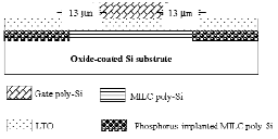
FIGURE 1 — Schematic cross-section of a Type G TFT.
Crystallization of amorphous-Si films by pulsed YAG2ω green laser for polycrystalline-Si TFT fabrication
Shinsuke Yura, Atsuhiro Sono,
Tatsuki Okamoto, Yukio Sato,
Tetsuo Kojima, Junichi Nishimae,
Mitsuo Inoue, Kaoru Motonami
Mitsubishi Electric Corp.
Abstract — A pulsed YAG2ω green laser with a line-shaped beam was applied in the crystallization process to fabricate polycrystalline-Si TFTs, and this procedure was compared with excimer-laser annealing (ELA). YAG2ω lasers are superior to excimer lasers in that they have fewer items to maintain and a longer working-time ratio. The crystallization mechanism for YAG2ω laser annealing (YLA) based on the lateral growth of grain is different from that of ELA. Its fluence margin was obtained from the n-channel mobility measured from fabricated TFTs and was found to be twice as large as that for ELA. We also found that overlapping irradiation does not change the mobility of TFTs. This is because the distribution of grain size is almost the same as in non-overlapping regions. This suggests the possibility of overlapping irradiation in YLA.
Excimer-laser annealing (ELA) is commonly used to crystallize amorphous-Si (a-Si) in the low-temperature polycrystalline-Si (poly-Si) TFT fabrication process. However, ELA requires many items to be maintained in mass production because it is excited by exhausting high-pressure active halogen gas and UV light decomposes organic material on the optical components. ELA requires that the discharge gas has to be changed daily and the windows cleaned. It also requires long-term maintenance where discharge electrodes, gas purifiers, and thyratron switches need to be changed. These items are not only costly but also decrease the working time. YAG2ω lasers do not require daily maintenance. They are excited by laser diodes, and the green light does not decompose organic materials. Therefore, lower maintenance costs and a higher working time ratio are expected.
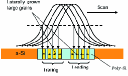
FIGURE 4 — Repeated irradiation.
Organic thin-film devices on paper substrates
Y. H. Kim
D. G. Moon
W. K. Kim
J. I. Han
Korea Electronics Technology Institute
Abstract — A high-performance polymer thin-film transistor fabricated on a paper substrate has been demonstrated. As a water barrier layer, parylene was coated on a paper substrate by using a vacuum deposition process. Using poly (3-hexylthiophene) as an active layer, a polymer thin-film transistor with a field-effect mobility of up to 0.086 cm2/V-sec and an on/off ratio of 104 was achieved. The fabrication of a polymer thin-film transistor built on an inexpensive paper substrate is expected to open a channel for future applications in flexible and disposable electronics with extremely low cost.
The paper sheet used in this experiment is a commercially available photo-paper for ink-jet printing. Due to water absorption, the paper sheet is easily damaged during the wet chemical process. Thus, a barrier layer must be coated on the substrate in order to carry out the standard OTFT fabrication process. Commonly used thin-film deposition methods, such as sputtering, evaporation, and spin coating, provide films with reasonable quality. However, several deposition steps are required to deposit films on both sides of the substrate, and the process is rather complicated. The parylene coating process, compared to other deposition process, is very effective and is a simple process for coating the entire substrate in a single step.
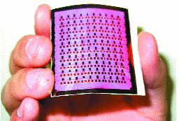
FIGURE 1 — Polymer thin-film-transistor array fabricated on a paper substrate.
Optical properties of solvent-cast polarizer films for liquid-crystal displays: A viscoelastic modeling framework
Jehuda Greener
Herong Lei
James Elman
Janglin Chen
Eastman Kodak Co.
Abstract — Many of the films used in polarizer assemblies in LCDs (
e.g., triacetyl cellulose or TAC) are produced by a solvent-casting process, which is known to impart optical anisotropy to the film expressed as finite out-of-plane birefringence. This feature of the film could have a significant impact on the optical performance of the display and it needs to be accounted for in any compensation scheme for the LC cell. This paper reviews the origin of this optical anisotropy, and it presents a viscoelastic model that links this property to the solvent-casting process and tosome key material parameters. The model results are compared with experimental data generated for polystyrene films cast from toluene, and generally good agreement is demonstrated.
Prescribed levels of birefringence in the polarizer films can be used to improve the performance of the display through various compensation schemes, which must be adapted to the particular LC cell employed. However, if the birefringence is greater or lower than the desired value, it could degrade the contrast ratio and decrease the viewing angle throughout the screen. For this reason, materials with inherently low birefringence, such as solvent-cast (SC) triacetyl cellulose (TAC) film, have been used traditionally in polarizer assemblies, e.g., as cover sheets for the sensitive and relatively soft poly(vinyl alcohol) (PVA) polarizer layer. TAC film and other similar solvent-cast polymer films are transversely isotropic, i.e., they possess nearly zero in-plane birefringence (IPBR), but the corresponding out-of-plane birefringence (OPBR) is finite and its magnitude depends on a variety of material and process factors.
TABLE 1 — List of materials.
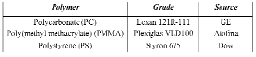
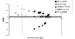
FIGURE 2 — OPBR (@λ = 590 nm) vs. dry film thickness for three polymer film types.
PFC emission-reduction strategy for the LCD industry
Hideki Nishida
Kunio Matsumura
Hideaki Kurokawa
Atsushi Hoshino
Seishi Masui
Hitachi Displays, Ltd.
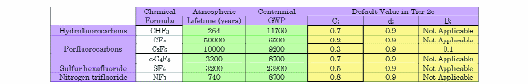
Abstract — The perfluorocarbons (PFCs) used as etching-process and chamber-cleaning gases in the manufacture of LCD devices have a high global-warming potential and a long atmospheric lifetime. Thus, to voluntarily reduce these environmentally harmful PFCs, in 2001 the Japanese LCD association established the World LCD Industry Cooperation Committee (WLICC), together with its counterpart associations in the Republic of Korea and Taiwan. Since that time involving many discussions, the WLICC reached a consensus on reducing the aggregate absolute PFC emissions to the equivalent of less than 0.82 million metric tons of carbon by 2010. Each association has been taking whatever emission reduction steps it considers best to achieve this goal. Thanks to these measures, the PFC emissions from the Japanese LCD industry have remained at the same level, or less, than those of the year 2000, in spite of the fact that PFC purchases have continually increased. In the interim, the Japanese LCD association has been obtaining experimental data for the 2006 IPCC Inventory Guidelines, which will give the emission factors needed to estimate the PFC emissions. As a result, some data are quite different from emission factors given in the current 2000 Inventory Guidelines. All the data obtained have been submitted to the IPCC to be adopted in the new 2006 Guidelines.
TABLE 1 — Properties of PFCs used for LCD manufacturing and emission factors stated in the current 2000 Guidelines.
Heat distribution in AMOLEDs
Ronald S. Cok
Jesse Coleman
Felipe Leon
James Mazzarella
Eastman Kodak Co.
Abstract — Thermal models and tests of active-matrix OLEDs (AMOLEDs) show that thermal effects can significantly reduce the lifetime of an OLED device. A comparison of the experimental heat distribution in an AMOLED with thermal models demonstrates that the thermal resistivity of the organic layers in an OLED is surprisingly high. Experiments with AMOLEDs show that the lifetime of OLED devices can be significantly improved through the use of heat-spreading layers in the OLED devices.
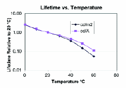
FIGURE 1 —Relative lifetime vs. OLED temperature normalized to 20°C.
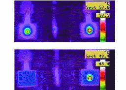
FIGURE 6 — Thermal images of a cover (left) and a substrate (right) of an AMOLED device in use without a metal heat spreader (top) and with a metal heat spreader (bottom).
Efficient and bright blue-emitting phosphorescent materials
Shi-Jay Yeh
Chin-Ti Chen
Yi-Hwa Song
Yun Chi
Meng-Huan Ho
Academia Sinica
Abstract — A new type of ancillary ligand for blue-emitting heteroleptic iridium complexes has been successfully developed. New ligands, 3-(trifluoromethyl)-5-(pyridin-2-yl)-1,2,4-triazolate and 5-(pyridin-2-yl)-tetrazolate, show stronger blue-shifting power than that of the picolate of FIrpic [iridium(III) bis(4,6-difluorophenylpyridinato)picolate]. Organic light-emitting diodes (OLEDs) fabricated with a new complex, FIrtaz [iridium (III) bis(4,6-difluorophenylpyridinato)(5-(pyridine-2-yl)-1,2,4-triazo-late) or FIrN4 [(iridium (III) bis(4,6-difluorophenylpyridinato)(5-(pyridin-2-yl)-tetrazolate], as the blue dopant in the host of mCP [1,3-bis(9-carbazolyl)benzene], exhibit near-saturated blue electrophosphorescence with Commision Internale de l'Eclairage (CIEx,y) coordinates of (0.14, 0.18) and (0.15, 0.24), respectively.
Photoluminescence spectra of FIrtaz and FIrN4 have shown very similar spectra pattern with the highest energy emission peak maximum located at 459 or 460 nm, which is about 10 nm blue-shifted from the 470 nm of FIrpic. Similar blue-shifting (ca. 5 nm) was also observed for the long-wavelength emission side bands of FIrtaz and FIrN4. As a result, both FIrtaz and FIrN4 showed noticeably blue photoluminescence (PL) in comparison with the greenish-blue color of FIrpic in CH2Cl2 solution at room temperature as pictured in quartz curvets excited with a UV lamp in Fig. 2.
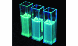
FIGURE 2 — Solution (CH2Cl2) photoluminescence images of FIrpic (left), FIrtaz (center), and FIrN4 (right).
A novel electron-transport material for organic light-emitting devices
Tswen-Hsin Liu
Jiin-Jou Lih
Au Optronics Corp.
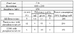
Abstract — A nanocrystalline electron-transport material [ET68] was introduced into organic light-emitting devices (OLEDs). By integrating a
p-doped transport system and phosphorescent emitters, a very bright and stable device could be obtained. Furthermore, 40% savings in power consumption can be achieved when the efficient pixels with ET68 were applied to AMOLEDs.
Since the major application of OLED panels is still mobile electronics at present, low power consumption is an important requirement for the application. Moreover, most of the novel OLED device architectures, such as tandem, top-emission, inverted structure, and phosphorescent emitters, will require higher operating voltages. In the mean time, to lower the operational voltage by using a good carrier transport/injection material is still a major challenge for OLED R&D. In this study, an effective and practical solution to approach this goal is provided and hopefully to meet the pressing need to reduce the voltage in OLEDs.
TABLE 1 — Power consumption comparison between 2-in. full-color AMOLED panels.
Blue-to-red electroluminescence from organic light-emitting field-effect transistor using various organic semiconductor materials
Takahito Oyamada
Hiroyuki Uchiuzou
Hiroyuki Sasabe
Chihaya Adachi
Chitose Institute of Science and Technology
Abstract — We succeeded in observing visible bright electroluminescence from blue to red in an organic field-effect-transistor structure. In particular, tetraphenylpyrene (TPPy) demonstrated a high photoluminescence efficiency of φPL ~ 70% and a maximum electroluminescence efficiency of ηEL ~10–2%. The electroluminescence efficiency (ηEL) was enhanced by using a short source-to-drain channel length (LSD < 1 μm). In addition, doping the TPPy layer with highly fluorescent rubrene molecules led to an φPL of ~100% and a maximum ηEL of 0.8%.
To date, the fabrication of OLEFETs using tetracene, fluorene-based polymer, MEH-PPV (Poly[2-methoxy-5-(2¢-ethylhexyloxy)-1,4-phenylenevinylene]), carbon nanotubes, and thiophene derivatives, has been reported. However, the use of these materials for OLEFETs has resulted in very low EL efficiency (ηEL < 10–3%). In these devices, the EL occurs around the drain electrodes because these materials basically have hole-accumulation characteristics. In addition, the operating source–drain (VSD) and gate (Vg)voltages, are all rather high (~100 V), while low operating voltages are required. In this study, therefore, we explored the ability of various organic semiconductor materials to produce the desired OLEFET characteristics.
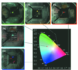
FIGURE 5 — Photographs of visible-light emissions in OLEFET with various organic semiconductor materials as active layers and CIE coordinates. (a) qTPD (x = 0.154, y = 0.075), (b) BSB: F8-TFB (x = 0.239, y = 0.482), (c) F8T2 (x = 0.388, y = 0.595), (d) rubrene:TPPy (x = 0.510, y = 0.480), and (e) PtOEP:F8TFB (x = 0.687, y =0.276).
3-D mobile display based on dual-directional light guides with a fast-switching liquid-crystal panel
Yu-Mioun Chu
Ko-Wei Chien
Han-Ping D. Shieh
Jim-Min Chang
Aaron Hu
Yi-Cheng Shiu
Vincent Yang
National Chiao Tung University
Abstract — An autostereoscopic display based on dual-directional light guides with a fast-switching liquid-crystal panel was designed and fabricated to provide better 3-D perception with image qualities comparable to that of 2-D displays. With two identical micro-grooved light guides, each with a light-controlled ability in one direction, two restricted viewing cones are formed to project pairs of parallax images to the viewer's respective eyes sequentially. Crosstalk of less than 10% located within ±8°–±30° and an LC response time of 7.1 msec for a 1.8-in. LCD panel can yield acceptable 3-D perceptions at a viewing distance of 5.6–23 cm. Moreover, 2-D/3-D compatibility is provided in this module.
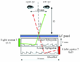
FIGURE 1 — Schematic of a dual directional light guide with a fast-switching LC panel and the relationship between the viewing angle and viewing distance, D ~ 32.5/tan θ (mm). D: viewing distance; θ: viewing angle (or inclination angle).
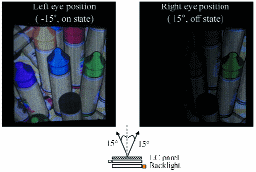
FIGURE 6 — Demonstration of a dual-directional backlight with an LC panel on the top, viewed at the positions of left eye and right eye, respectively, to show the distinguished directionality for a time-multiplexed 3D display.