Flexible Transistor Arrays
Markets are now emerging for flexible transistor arrays and the state of the art is exciting, but there are challenges to be overcome before flexible arrays can enter the mainstream.
by Peter Smith, David Allee, Curt Moyer, and Douglas Loy
FLEXIBLE switch-transistor arrays will be necessary for fabricating active-matrix flexible displays as well as a variety of large-area electronics currently envisioned for plastic or flexible substrates. Transistors are currently used as switches, but with markets now emerging for flexible transistor arrays, it is time to provide definitions, examples, and technology options, and to suggest solutions to the known challenges.
The "flexible transistor array" has several definitions. The simplest level of flexibility is found in a device that can be conformed once to a surface curved in one axis. This simplest level of flexibility requires films that do not reside at the neutral axis of the backplane to stretch or compress in one direction one time without failure. Deforming an array one time in two axes requires the array to be stretched in two axes, which yields a trapezoidal surface deformation and a second level of flexibility.
An array that can be repeatedly flexed in one axis adds a robustness requirement and a third level of flexibility. A fourth level of flexibility is an array capable of repeated flexing in two axes, which, in the extreme, would be a foldable device. The amount of flexing each array structure can tolerate depends on the stiffness of the substrate, the rigidity of the structure, and the rigidity of the surrounding structures.
Some currently envisioned flexible displays employ transistor arrays and one of several electro-optic technologies, including electrophoretic ink, cholesteric liquid crystal, and organic light-emitting diodes (OLEDs). Electrophoretic and cholesteric displays are top-reflective and require voltages up to 80 V for optimal operation. They also require thick dielectric layers to reduce capacitive coupling. The OLED display, on the other hand, is typically bottom-emitting and operates at lower voltages with thinner dielectrics. Therefore, the requirements placed upon the transistor technology depend upon the electro-optic approach being used.
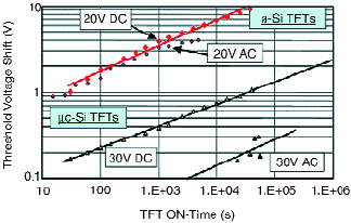
Fig. 1: The threshold-voltage shift is shown as a function of the stressing time at 60°C under dc or ac gate voltage. The threshold-voltage shift for microcrystalline-silicon TFTs is relatively small, in particular under ac stress. [See P. Roca i Cabarrocas et al., J. Soc. Info. Display 12, No. 1, 3–9 (2004).]
Regardless of the electro-optic technology utilized, the backplane-technology options include inorganic and organic semiconductors. We will review these options with an eye toward fabrication on plastic flexible substrates and discuss emerging array tech-nologies such as nanocrystalline Si and composite nanowires. Flexible glass and stainless steel are viable alternatives but will not be discussed here. (For information on stainless-steel substrates, see the article by Vincent Cannella et al. in this issue. – Ed.)
Amorphous Silicon
Amorphous-silicon thin-film-transistor (a-Si TFT) technology is a mature approach for glass substrates. The extension of a-Si TFTs to flexible plastic substrates requires
• The reduction of fabrication temperatures to about 150°C (for PEN plastic, as an example),
• Adequate encapsulation and purity of thesubstrate material to control mobile ions and the reliability issues that derive from them,
• Adequate moisture content,
• Creep and thermal-expansion control of the substrate during processing to prevent dimensional shifts that compromise align-ment tolerances, which need to be kept to 1 ppm, and
• Adequate adhesion of device layers during processing and over the device's lifetime.
As a first step, the goal of a-Si TFTs on flexible plastic substrates is to achieve equivalent performance to a-Si TFTs on glass substrates. On glass, the threshold voltage and current-matching of a-Si TFTs across an array is much better than that of polysilicon (poly-Si) TFTs. Off-state leakage currents in the subpicoamp range with on currents in the microamp range are typical of a-Si TFTs. TFTs in LCD pixels must have on/off current ratios greater than 106, a requirement that is reliably met by today's a-Si TFTs.
Unfortunately, the threshold voltages of a-Si TFTs drift rapidly during operation, with as much as a 3-V increase in a few hours (Fig. 1). But TFTs in commercial active-matrix liquid-crystal-display (AMLCD) pixels are used as switches, so the threshold-voltage shift can be compensated by overdriving the gate – usually the row line – sufficiently to fully switch the a-Si TFT at projected end-of-life. There is, however, a price to be paid for this solution. Overdriving the gate accelerates the threshold drift rate, leads to higher power dissipation (proportional to V2), and increases the undesirable charge shift (C x V) in the storage capacitor through the parasitic TFT capacitance.
The threshold-voltage shift over time makes it harder to implement peripheral analog drive circuitry, such as AMLCD column drivers, on the a-Si TFT glass. Similarly, active-matrix OLED arrays have an analog current drive. The simple two-transistor pixel circuit for driving OLEDs requires active sensing and column-drive adjustment to compensate for the threshold-voltage shift. Alternatively, OLED pixel circuits with higher transistor counts and current-referenced drive have sometimes been used in combination with reverse-biasing drive schemes to compensate and limit the threshold-voltage shift. But the high pixel-transistor counts and additional bus lines in such designs have a direct impact on TFT-array yield.
The parasitic capacitance of TFTs can be reduced by a higher carrier mobility, which permits the use of narrower transistor widths. This is one of the motivations for using polysilicon. Typical a-Si active-layer mobility is below 1 cm2/V-sec.
Polycrystalline Silicon
The electron mobility of poly-Si TFTs is markedly higher than that of a-Si TFTs (200 vs. 1 cm2/V-sec). The higher mobility is achieved by recrystallizing the deposited a-Si by laser annealing. But the mobility is still several times lower than the 1000 cm2/V-sec that is readily achieved in single-crystal silicon (x-Si).
Another advantage is that CMOS circuits can be made in poly-Si because it is possible to fabricate both N-and P-type TFTs. Since CMOS is the dominant technology in the integrated-circuit (IC) industry, there is substantial experience in designing sophisticated integrated circuitry in CMOS. In stark contrast, only N-type transistors are possible in a-Si, making circuit design more complicated. N-type-only circuits have not been widely built in the IC industry since the 1970s, although N-type active-matrix backplanes are the mainstay of the display industry.
Table 1: Comparison of TFTs
| |
Amorphous silicon |
Polycrystalline silicon |
Microcrystalline silicon |
Organic thin film |
| Status |
Mature |
Development |
Research |
Research |
| TFT type |
NFET |
NFET and PFET |
NFET |
O-TFT |
| Mobility (cm2/V-sec) |
0.1–1.0 |
50–200 |
Top gate: 1–30
Bottom gate: ~3
|
0.005–1.5 |
| Uniformity |
Good |
Poor |
Unknown |
Unknown |
| Stability |
Poor |
Good |
Good |
Unknown |
| Cost |
Low |
High |
Low |
Very Low |
| Ion/Ioff |
>106 |
>106 |
>106 |
103–108 |
Size and voltage to drive 10 μA
(Gate dielectric is 300 nm
and gate length is 5 μm) |
W = 92 μm
(Vgs – Vt) = 7 V |
W = 10 μm
(Vgs – Vt) = 1.5 V |
W = 9.4 μm
(Vgs – Vt) = 4 V |
W = 181 μm
(Vgs – Vt) = 25 V
|
| Unity-gain frequency (MHz) |
4.5 (Vgs – Vt) = 7 V |
191 (Vgs – Vt) = 1.5 V |
76 (Vgs – Vt) = 4 V |
1.6 (Vgs – Vt) = 25 V |
Significantly, poly-Si TFTs have good stability over time, quite unlike a-Si TFTs. The inherent stability of poly-Si takes on greater importance as the process temperature is reduced for flexible-substrate compatibility. As discussed previously, the threshold, or turn-on, voltage for a-Si TFTs rises continuously with electrical stress, increasing many volts with extended use. Poly-Si TFTs do not experience this shift in threshold voltage, and thus avoid a serious reliability problem. This fundamental difference is widened as the substrate moves from glass to plastic.
But poly-Si technology has suffered from poor spatial uniformity. While many transistors in an array will have excellent performance, a few will have very low mobility because of the random positioning of a grain boundary across a device channel.
A typical transistor array has many thousands or millions of transistors, but a single bad pixel in a display can be readily visible. Limited redundancy can be incorporated into the design of some circuits, but spatial uniformity remains a critical problem. Research is currently under way to improve poly-Si uniformity by lateral recrystallization of the silicon. The goal is to produce elongated grains stretching from the source to the drain of each TFT, thereby minimizing the likelihood of a grain-boundary intersection in the current path.
Let us compare the performance of poly-Si with a-Si. In active-matrix backplanes, a figure of merit is the width of device necessary to carry 10 A of current. A smaller device enables a greater fill factor and higher-resolution displays.
Using the standard equation for saturation current in a field-effect transistor (FET), a 10-μm-wide poly-Si TFT with a gate overdrive voltage of 1.5 V will carry 10 μA (a 300-nm silicon nitride gate dielectric and a 5-μm gate length are assumed). The gate overdrive voltage is set to one-half the power-supply voltage, 5 V, less the typical threshold voltage of 1 V. Under similar conditions, an a-Si TFT with a typical power-supply voltage of 20 V requires a device 92 μm wide to carry 10 μA (the typical threshold voltage was assumed to be 3 V). In both cases, the highest reported mobility was used. The conclusion is that an a-Si TFT has to be nine times larger to carry the same current, even when a higher power supply voltage partly compensates for the low mobility. This size difference can be significant in high-resolution displays.
For digital and analog circuits generally, the unity-gain frequency is a common figure of merit. The unity-gain frequency is equal to the device transconductance divided by the gate capacitance. Equivalently, it is proportional to device mobility and gate overdrive voltage, and inversely proportional to the square of the gate length.
Experience with other crystalline semicon-ductors suggests that useful circuits can be built up to one-tenth of the unity-gain frequency. Results may be somewhat worse for TFTs because of the large parasitic capacitances. The unity-gain frequency for poly-Si TFTs is 191 vs. 4.5 MHz for a-Si TFTs. This suggests that circuits operating around 10 MHz are possible for poly-Si, but a-Si is limited to approximately 100 kHz (Table 1).

 Nanosys
Fig. 2: Nanowire transistors use nanometer-thick single-crystal conductors that have very high carrier mobility (left). Because many different nanowires span the source and drain electrodes in a nanowire TFT (see micrograph, right), the technology avoids the occasional low mobility found in poly-Si TFTs due to the random positioning of a grain boundary across a device channel.
Organic TFTs
Organic TFTs can be fabricated from conjugated polymers, oligomers, or small-molecule organics. Mobilities as high as 1.5 cm2/V-sec with an on/off current ratio of 108 have been obtained using pentacene as the active semi-conducting layer. Carrier mobilities in polymer-based TFTs have varied between 5 x 10⁻³ and 0.1 cm2/V-sec. Higher mobilities in small-molecule-based TFTs have been attributed to the quality of molecular ordering within the films. But small molecules, such as pentacene, require vacuum deposition to obtain high-quality films with long-range molecular ordering. Polymer-based TFTs offer the advantage of solution processing, which may be beneficial because of lower-cost manufacturing.
The active layer in polymer TFTs may be fabricated with conjugated polymers such as polyacetylene, polythiophene, polypyrrole, and poly(thienylene-vinylene). Polymers offer the advantage of ink-jet-printing or spin-casting fabrication methods, but a remaining obstacle is obtaining pure materials and well-ordered films. Purity defects in the material may give rise to charge-trapping sites that decrease conductive efficiency.
Charge transport in conducting polymers is quite complex and involves a very efficient mechanism of transport along the intrachain-conjugated backbone. This efficient mechanism is interrupted by an inefficient interchain hopping of the charge to adjacent chains induced by defective ordering.
Film orientation and uniformity are key factors in producing highly conductive, thin organic films. Recent research, therefore, has been focused on finding methods of obtaining active layers with the preferred molecular orientation and ordering. Different substrates have been chosen to induce ordering of organic thin films. P. Lang of the Laboratoire des Matériaux Moléculaires, CNRS, Thiais, France, along with colleagues at the Institut Charles Sadron, Strasbourg, France, and CECM, Vitry, France, reported that sexithiophene (-6T) thin films vacuum-deposited on SiH/Si substrates preferentially orders its molecular axis parallel to the substrate, while it is preferentially oriented perpendicular to the surface when SiO2 is used as the substrate.
Other researchers have tried polymer substrates or pretreating SiO2 substrates with polymers, such as polytetrafluoroethylene, to induce the desired orientation and molecular ordering. Another method to induce a specific orientation involves using an applied electric field during the epitaxial growth of organic crystals. Annealing of the film has also been used to control film structure and morphology. Although these methods have improved film performance to some extent, the quality and fabrication processes are still not practical for commercial applications.
Stability varies significantly depending on the organic material. Some organic films, and particularly organic electrode interfaces, are very sensitive to moisture and oxygen. Spatial uniformity is not well understood at this early stage of research. However, Philips has built a complete set of row drivers for a display incorporating a few thousand transistors. The very low mobility is partly compensated by a high power-supply voltage of 60 V. Assuming a 300-nm gate dielectric with a relative permittivity of 3, and using a 5-μm gate length, a 181-μm-wide device is necessary to carry 10 μA of current. A unity-gain frequency of 1.6 MHz suggests that useful digital and analog circuits could operate at several tens of kHz.
Emerging Materials
Microcrystalline silicon is obtained by adjusting the plasma-deposition conditions in the a-Si process. Either top- or bottom-gate N-type TFTs can be fabricated. Microcrystalline materials have been grown at less than 250°C, which is approaching temperatures compatible with plastic substrates. Successful production of microcrystalline silicon at plastic-compatible temperatures would permit the implementation of higher-speed, lower-capacitance, more-stable, and analog-capable flexible TFT arrays.
Bottom-gate microcrystalline TFTs have achieved an electron mobility of 3 cm2/V-sec, a small but significant improvement over a-Si. Top-gate TFTs have achieved electron mobilities up to 30 cm2/V-sec, a substantial improvement. The bottom-gate process is compatible with the existing a-Si process. Most importantly, microcrystalline TFTs are about ten times as stable as a-Si TFTs over time.
 Rolltronics
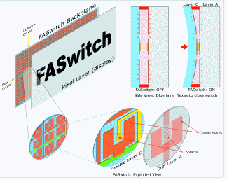
Fig. 3: Rolltronics has developed a microelectromechanical switch that could replace the TFT as a pixel switch for flexible displays. FASwitch technology uses charged electrostatic plates to deform a plastic membrane that closes a physical contact. It can be produced by the same tools and processes that are used in the flexible-circuit-board industry.
With all of the limitations of silicon- and organic-transistor technologies, several companies are focusing on emerging material technologies that may allow them to do an end run around the problems of organic- and silicon-based technologies. These companies include Nanosys, Versatilis, and Cambrios.
Nanosys has the ability to manufacture nanometer-sized fibers (or wires) made of single-crystal semiconductors such as silicon (Fig. 2). These "nanowire" transistors can be coated onto substrates such as glass or plastic as a low-temperature alternative to poly-Si. Integrating this inherently flexible structure between a source and drain into the full fabrication process would permit previously inconceivable device performance while removing thermal-process limitations originating in the substrate.
Versatilis is focusing on layer-transfer techniques as the best way to realize high-performance TFT arrays on flexible substrates.
Cambrios is contemplating room-temperature fabrication of poly-Si channel structures via protein-template synthesis and integrating the process into the existing TFT infrastructure.
Each of these early stage corporate technologies offers solutions to known problems; the timeline for their adoption is predicated on solving problems associated with scalability and market requirements that change with time.
Finally, Rolltronics has demonstrated an architecture that may obviate the need for either the organic- or inorganic-transistor technologies discussed above. While transistors have traditionally served the role of switches in an active matrix, Rolltronics has developed an alternative in the form of a microelectromechanical switch (Fig. 3). Composed mainly of plastic and metals, it can be produced by the same tools and processes that are used in the flexible-circuit-board industry.
Rolltronics's FASwitch technology uses charged electrostatic plates to deform a plastic membrane that closes a physical contact. The switch circuit is separate from the drive circuit. FASwitch can be used to power either voltage- or current-driven devices, may be momentary or latched, and may switch either ac or dc at high or low voltages.
The Challenges Ahead
Arizona State University's Flexible Display Center – the largest flexible-display center in the U.S. – has chosen to focus on the scalability of a-Si, a technology that presumably poses the least amount of technical difficulty at the outset. A natural next step for the Center is the exploration of multicrystalline silicon.
Multinational companies are exploring these and other options. Because the interplay of substrate, semiconductor, electro-optic function, manufacturing technology, and application is extremely complex, developing a combination of technologies that successfully implements a flexible switch array and resulting display requires the placing of several bets. The challenge does not reside in a single choice of switch technology, but more in the full integration of the components required to serve the emerging flexible-display and macroelectronic marketplace. •
Peter Smith, David Allee, Curt Moyer, and Douglas Loy are with the Flexible Display Center at Arizona State University, 7700 S. River Pkwy., Tempe, AZ 85284; telephone 480/727-8941, e-mail: peter.smith@asu.edu. The authors are pleased to acknowledge contributions to this article by the U.S. Army Research Laboratory, Philips, Kent Displays, Inc., E Ink Corp., Universal Display Corp., Honeywell, Penn State University, Lucent, the University of Waterloo, and Kyoto University. The Flexible Display Center is sponsored by the Army Research Laboratory under Cooperative Agreement Number W911NF-04-2-0005.