A preview of the papers appearing in the July 2005 issue of the Journal of the SID, available on-line at www.SID.org.
Edited by Aris Silzars
Oxide engineering of ZnO thin-film transistors for flexible electronics
P. F. Carcia
R. S. McLean
M. H. Reilly
DuPont Research and DevelopmentExperimental Station
Abstract — In this paper, it is shown that ZnO thin-film transistors (TFTs) are potentially a higher performance alternative to organic and amorphous-Si TFTs for macroelectronics on plastic substrates. Specifically, nanocrystalline ZnO thin-film transistors using low-temperature processing, compatible with flexible electronics on plastic substrates, were fabricated. The ZnO semiconductor was rf magnetron sputtered, and the Al2O3 gate dielectric was deposited either by electron-beam evaporation or atomic layer deposition. By controlling the partial pressure of oxygen (pO2) during ZnO sputtering, the field-effect mobility of ZnO transistors can be engineered to be between 2 and 42 cm2/V-sec, attractive for high-performance electronic applications. It is contended that pO2controls the oxygen-vacancy content or stoichiometry of ZnO, and that allows control of transistor field-effect mobility. Although most of the devices described here were fabricated on Si substrates, devices made on a thin (50 μm thick) polyimide substrate had about equivalent performance, affirming the compatibility of the processes with plastic substrates. Finally, it will be shown that properties of nanocrystalline ZnO transistors can be explained by transport models that account for grain-boundary trapping of mobile carriers.
ZnO TFTs on a flexible polyimide substrate (DuPont Kapton® 200EZ film) was fabricated by using metal shadow masks at each level of the device construction. First, the Al gate electrodes were thermally evaporated, followed by e-beam evaporation of the 400-nm-thick Al2O3 dielectric, then the Al source–drain electrodes, and finally 50 nm of sputtered ZnO semiconductor. Representative transfer and output characteristics for these initial ZnO TFTs with Al2O3 dielectric on flexible polyimide are shown in Fig. 14. The mobility of ~50 cm2/V-sec washigher than for comparable ZnO made at pO2 = 3 x 10⁻⁵ Torr of oxygen on Si, while the gate leakage current was only slightly higher, and the threshold voltage somewhat lower.
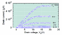
FIGURE 14 — Output current characteristic for ZnO TFT for drain voltages 0–20 V and gate step increment ΔVg =2 V for Vg = 0–10 V. Substrate is 50-μm-thick Kapton® polyimde film.
Process study and optimization for fabrication of poly-Si thin-film transistors on plastic substrates
Wonsuk Chung
Francesco Lemmi
Patrick M. Smith
Teruo Sasagawa
FlexICs, Inc.
Abstract — A complete poly-Si thin-film transistor (TFT) on plastic process has been optimized to produce TFT arrays for active-matrix displays. A detailed study of the poly-Si crystallization process, a mechanism for protecting the plastic substrate from the pulsed laser used to crystallize the silicon, and a high-performance low-temperature gate dielectric film is presented. Poly-Si grain sizes and the corresponding TFT performance have been measured for a range of excimer-laser crystallization fluences near the full-melt threshold, allowing optimization of the laser-crystallization process. A Bragg reflector stack has been embedded in the plastic coating layers; its effectiveness in protecting the plastic from the excimer-laser pulse is described. Finally, a plasma pre-oxidation step, which has been added to a low-temperature (<100°C) gate dielectric film deposition process to dramatically improve the electrical properties of the gate dielectric, is described. These processes have been integrated into a complete poly-Si TFT on plastic fabrication process, which produces PMOS TFTs with mobilities of 66 cm2/V-sec, threshold voltages of –3.5 V, and off currents of approximately 1 pA per micron of gate width.
Many research groups have extensively studied the mechanism of XeCl excimer-laser crystallization of amorphous silicon prepared by CVD. However, in this experiment, amorphous-silicon films prepared by ac sputtering system were used. As expected, measurements show that the dependence of grain size of sputtered silicon on the laser crystallization fluence exhibits characteristics similar to other work on CVD silicon, with two distinct regimes (the low- and high-fluence regimes) clearly discernable. In the low-fluence regime (<235 mJ/cm2), grain sizes increase slowly because the melt depth increases with increasing laser fluence. On the other hand, in the high-fluence regime (>235 mJ/cm2), grain size is not affected by variations in laser fluence because the crystallization mechanism is different.
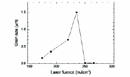
FIGURE 1 — Variation of average grain size (diameter) as a function of laser fluences.
Stress control for overlay registration in a-Si:H TFTs on flexible organic-polymer-foil substrates
I-Chun Cheng
Alexis Kattamis
Ke Long
James C. Sturm
Sigurd Wagner
Princeton University
Abstract — Mechanical stress in hydrogenated amorphous-silicon (a-Si:H) thin-film transistors (TFTs) is becoming an important design parameter, especially when the TFTs are made on compliant substrates. Excessive stress always has been avoided to prevent film fracture and peeling. Now, attention is turning to the effects of stress on the TFT backplane dimensions and hence on the overlay alignment. The goal is to keep the size of the circuit-on-substrate composite structure the same at successive critical photolithographic steps. This is done most easily by keeping the structure flat. It is shown that a compensating stress can be dialed into the silicon nitride (SiNx) gate dielectric to also keep the substrate size constant. Varying the stress in the SiNx gate dielectric did not significantly change the as-fabricated TFT characteristics.
Organic polymer foils are major substrate candidates for flexible electronics. They offer the advantages of light weight, transparency, flexibility, even deformability, and possibly low cost. However, organic polymers typically have high coefficients of thermal expansion, low elastic moduli, and low dimensional stability compared to conventional glass substrates. These characteristics bring with them challenges in overlay registration during device fabrication.
FIGURE 1 — Curvature induced by stress in films of (a) Cr and a-Si:H and (b) SiNx deposited over a range of RF power, all on 50-μm-thick Kapton® 200E polyimide substrates. All films are on the side of the substrate that faces left. The 300–500-nm-thick SiNx and the 250-nm-thick a-Si:H films were deposited at 150°C, and the 80-nm-thick Cr was deposited by thermal evaporation without control of substrate temperature. The built-in stress of Cr is tensile and that of a-Si:H is compressive. The built-in stress in SiNx can be adjusted by deposition power. The bare substrate has the radius of curvature R0.
A new method for measuring ultra-low water-vapor permeation for OLED displays
Ralf Dunkel
Roko Bujas
Andre Klein
Volker Horndt
General Atomics
Abstract — It is well known that proper encapsulation is crucial for the lifetime of organic light-emitting-diode (OLED) displays. With the development of increasingly better barrier coatings and perimeter seals, it has now become very desirable to be able to precisely measure the rate of water-vapor and oxygen permeation through barrier coatings and perimeter sealing. This paper demonstrates a new permeation-measurement method that uses tritium-containing water (HTO) as a tracer material. The theoretical detection limit of this direct method is 2.4 x 10⁻⁸g/(m2-day).
The most commonly used tools for measuring water-vapor and oxygen permeation through plastic films are instruments made for food packaging by MOCON, Inc. Their current detection limit is approximately 0.005 g/(m2-day) for water. There are many permeation-testing methods that have been developed recently. These methods use detection principles that are gravimetric, capacitive or resistive, spectroscopic, or based on calcium degradation. Here, a permeation measurement method and apparatus for measuring ultra-low water permeation are presented. This method uses tritium-enriched water (HTO) as a tracer material. The apparatus can be used to measure the permeability of polymer substrates with barrier coatings as well as the permeability of perimeter sealing for OLED displays.
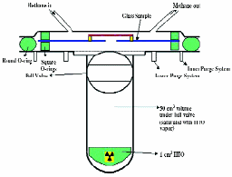
FIGURE 5 — Arrangement for testing perimeter sealing.
Development and evaluation of bend-testing techniques for flexible-display applications
Sonia Grego
Jay Lewis
Erik Vick
Dorota Temple
RTI International
Abstract — Two different approaches to automated bend testing of flexible substrates for display applications were implemented and characterized: a conventional collapsing radius geometry and a novel technique called the "X–Y–θ" geometry. Indium tin oxide (ITO) coated polymer substrates were used to compare the performance of the two automated systems by in-situ electrical-resistance measurements. Manual bending on fixed-diameter mandrels was used to help interpret the results. The advantages and drawbacks of the two systems for providing information of practical use to flexible display R&D are discussed.
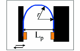
FIGURE 1 — Schematic of collapsing radius apparatus.
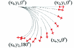
FIGURE 2 — Schematic of the bending geometry in the X–Y–θ system.
A scalable manufacturing process for flexible active-matrix e-paper displays
S. E. Burns, et al.
Plastic Logic, Ltd.
Abstract — A scalable manufacturing process for fabricating active-matrix backplanes on low-cost flexible substrates, a key enabler for electronic-paper displays, is presented. This process is based on solution processing, ink-jet printing, and laser patterning. A multilayer architecture is employed to enable high aperture ratio and array performance. These backplanes were combined with E Ink electrophoretic media to create high-performance displays that have high contrast, are bistable, and can be flexed repeatedly to a radius of curvature of 5 mm.
The TFTs are formed in a top-gate configuration on a 125-μm-thick planarized PET substrate with a polyfluorene-based polymer semiconductor (SC) and a spin-coated polymer dielectric. After ink-jet printing a silver gate electrode, an organic dielectric layer with a thickness of 10 μm is deposited. Then via-hole interconnections are defined by laser ablation through the layer stack, exposing the buried TFT drain electrode on the substrate. A pixel electrode of the conducting polymer poly(3,4-ethylene dioxythiophene)/poly(styrene sulfonate) (PEDOT/ PSS) is deposited by ink-jet printing. During this step, the top pixel electrode is electrically connected to the TFT drain electrode. Subsequently, the substrate is laminated with an E Ink® Imaging Film on top of an ITO counter-electrode on a second PETsubstrate.
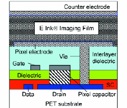
FIGURE 1 – Cross-sectional view of the novel multilayer pixel architecture.
Pixel circuits and drive schemes for glass and elastic AMOLED displays
S. Alexander, P. Servati,
G. R. Chaji, S. Ashtiani,
R. Huang, D. Striakhilev,
K. Sakariya, A. Kumar,
A.Nathan,C.Church,
J. Wzorek, P. Arsenault
Ignis Innovation, Inc.
Abstract — Flexible AMOLED displays pose unique opportunities and challenges for a-Si. Leveraging the existing a-Si process infrastructure is the fastest and lowest-cost route to flexible AMOLEDs. However, the displays must maintain high performance, long lifetimes, and high uniformity despite low-temperature processes and mechanical stress. New pixel circuits and drive schemes shown here demonstrate that high-performance flexible AMOLED displays are possible using well-established a-Si technology.
An option to increase programming speed of current-programmed circuits is the proposed hybrid current–voltage programming scheme, where a circuit intended for current programming (such as Ignis's 4-T pixel) is programmed with a voltage. A block diagram is shown in Fig. 2. There are two modes of operation: normal operation and calibration. During normal operation, standard voltage programming is used. The display controller takes incoming video data, uses a look-up table to determine the correct voltage, and outputs the data to the standard LCD source driver. The switch matrix is configured to directly connect each of the outputs from the LCD driver to the data lines of the display. To re-calibrate, the switch matrix connects the current source to one column, and each pixel in that column is programmed (one at a time) with a current instead of a voltage. The voltage on the data line is recorded by an analog-to-digital converter (ADC) and stored in the look-up table.
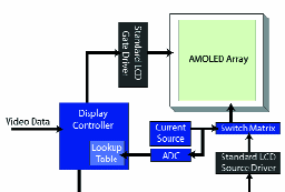
FIGURE 2 — Block diagram of hybrid drive scheme.
Novel alignment technique for liquid crystal using hydrophilic/hydrophobic pattern layer
A. Suemasu
K. Ikegami
N. Maji
T. Tanaka
Dai Nippon Printing Co., Ltd.
Abstract — A novel method of aligning liquid-crystal (LC) molecules that employs a layer patterned with hydrophilic and hydrophobic regions fabricated by the photocatalysis of TiO2 has been developed. This method provides a resolution on the order of 10 μm for the alignment of LC molecules without the need for protrusions or patterned electrodes. Using this method, the continuous multidomain vertical alignment of LC molecules was achieved.
LC cells were assembled from two substrates, one covered with hydro-philic and hydrophobic regions and the other coated with a hydrophobic layer. The cell gap was kept constant at 3.5 μm by using a spacer in the sealing material. Cells were filled with nematic LC (MLC-6608, Merck, Ltd.), which has a negative dielectric anisotropy. Moreover, dichromatic dye was added to the LC material so that the orientation of the LC molecules could be determined. Figure 6 shows microscope photographs taken through a linear polarizer of an LC cell with a zigzag hydrophilic/hydrophobic micropattern. The photomask used to make the cell contained right-angled zigzag patterns made up of 75-μm-wide chromium lines and 25-μm-wide spaces. The figure shows that the LC molecules are aligned parallel to the lines of the pattern.
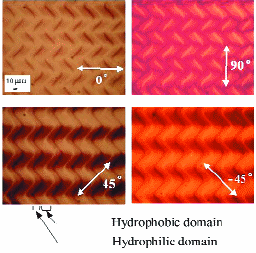
FIGURE 6 — Microscope photographs of zigzag hydrophilic/ hydrophobic pattern under an applied voltage. (Arrow: Transmission axis of polarizer.)
Liquid-crystal displays using printed plastic TFT backplanes
T. Wilkinson
S. Ward-Foxton
A. Menon
W. H. Reeves
S. E. Burns
Cambridge University
Abstract — In this paper, results from a new liquid crystal over plastic printed thin-film-transistor (TFT) display is presented. The display demonstrator shows that the processing incompatibilities between the plastic TFT backplane and the liquid-crystal materials can be addressed to make a stable twisted-nematic structure. New fabrication processes such as the photo-alignment of liquid crystals have made it possible to create a new generation of displays, which pave the way towards fully integrated plastic liquid-crystal-display technologies.
The ink-jet-printed organic polymer TFT active-matrix backplanes are produced using a solution processing of semiconductors, dielectrics, and conductors. A high device yield, uniformity, and resolution required for thin-film electronics applications can be achieved by using a combination of surface-energy patterning and ink-jet printing (Fig. 1). In this process, the critical TFT channel length is fabricated by patterning the surface energy of the substrate prior to printing the transistor source and drain. This allows channel lengths of 10 μm to be consistently defined although submicron definition has also been demonstrated.
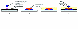
FIGURE 1 — The main process steps in fabricating our TFTs.