A preview of the papers appearing in the January 2005 issue of the Journal of the SID, available on-line at www.SID.org.
Edited by Aris Silzars
Fully digital LCoS device for consumer applications
Shigeo Shimizu
Yutaka Ochi
Atsushi Nakano
Matthew Bone
Abstract — This paper presents a new display device, which combines a digital backplane and a vertically aligned nematic liquid-crystal layer. The device has 1280 x 720 pixels in a 0.7-in.-diagonal display area. The concept of the new device will be presented and the performance of the device for a rear-projection television application will be reviewed.
Keywords — D-ILA, LCoS, rear-projection TV, digital driving.
D-ILA is a type of LCoS device and has superior features such as high contrast ratio, high efficiency, smooth image, and high reliability under intense illumination light. But thus far, D-ILA has been limited to high-end professional applications. The new 720P device is targeted at consumer applications and employs a fully digital driving method. The fundamental device structure is the same as the conventional D-ILA. The device consists of a glass substrate and a silicon backplane and between them a liquid-crystal layer. The liquid crystal we used was a negative dielectric anisotropy nematic type, which is aligned vertically (VAN mode) and is designed to respond to the average RMS voltage of the pulse-width modulation (PWM) signal. Its diagonal is 0.70 in., the pixel pitch is 12 μm, and there are 1280 x 720 pixels in the display area. The electrical addressing employs a PWM driving method. The fill factor of the device is nearly 93%, which is designed to produce a smooth bright image.
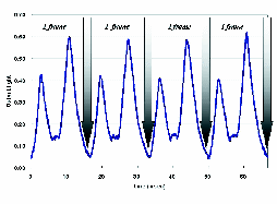
FIGURE 10 – Measured output light response at 128 gray levels.
Towards large-area full-color active-matrix printed polymer OLED television
N. C. van der Vaart, H. Lifka,
F. P. M. Budzelaar, J. E. J. M. Rubingh,
J. J. L. Hoppenbrouwers,
J. F. Dijksman, R. G. F. A. Verbeek,
R. van Woudenberg,
F. J. Vossen, M. G. H. Hiddink,
J. J. W. M. Rosink, T. N. M. Bernards,
A. Giraldo, N. D. Young,
D. A. Fish, M. J. Childs,
W. A. Steer, D. Lee, D. S. George
Abstract — A new multi-head polymer OLED ink-jet-printing technology to make large-screen OLED television displays has been developed. This printer was used to make a 13-in.-diagonal 16:9-format polymer-OLED prototype driven by an LTPS active matrix with a pixel circuit which compensates for TFT threshold-voltage variations. A novel scrolling-bar addressing scheme was used to reduce motion artifacts and to make sparkling images with a high local peak brightness. The scalability of the polymer-OLED technology to larger sizes for television applications will be discussed.
Keywords — OLED, PolyLED, active matrix, ink-jet printing.
The objective of this paper is to demonstrate an inexpensive method of making large-panel OLED television displays. Ink-jet printing was used to deposit polymer OLED (PLED) materials, which is easily scalable to large-screen diagonals. An important application in the large-TV segment is a wide-screen display with a 30-in. diagonal and high-definition TV resolution. This display was chosen as a reference application and a 13-in. version was made as part of a 30-in. display with WXGA resolution (1365 x 768). A 13-in. carve-out then yields a 576 x 324 resolution. By using this panel, the complete display chain from active-matrix design and fabrication through PLED panel fabrication, driver electronics, and display-specific video processing to display perception aspects were investigated.
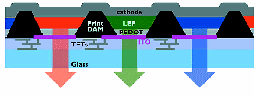
FIGURE 1 – Cross section of polymer OLED pixel structure.
Current status and future prospect of in-cell-polarizer technology
Y. Ukai, T. Ohyama,
L. Fennell, Y. Kato,
M. Paukshto, P. Smith,
O. Yamashita, S. Nakanishi
Abstract — A thin-crystalline-film (TCF) polarizer has been developed, which can be used internally in liquid-crystal-display cells. Based on this material, a manufacturing process has been developed for the fabrication of monochrome LCDs with internal polarizers. A new TCF polarizer material and coating equipment, developed to realize a high-performance color TFT-LCD, are discussed.
Keywords — In-cell polarizer, TFT-LCD, transflective, lyotropic liquid-crystal die.
In this paper, the possibility of incorporating the polarizer within the LCD cell was examined. In order to solve the drawbacks of conventional transmissive and transflective LCDs, single TN-mode TFT-LCDs with an in-cell polarizer that realizes high transmittance and a high level of visibility under ambient light was developed. The typical TCF is formed by molecules with molecular dimensions of 2–3 nm in plane and with 0.34-nm thickness for the plate-like molecule. The typical functional layer has a thickness from about 60 up to 1000 nm, which means that it has from 20 up to 300 molecular layers that form an optically anisotropic film. The absorption dipoles are located in the molecular plane such that the direction perpendicular to the disk-shaped molecules is the transmission direction.
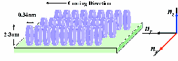
FIGURE 1 – One molecular layer of TCF coating.
The 121-contiguous-subfield addressing of high Xe-content PDPs
A. Saito
T. Maeda
M. Tone
T. Shiga
S. Mikoshiba
G. Oversluizen
Abstract — As the Xe content of PDPs is increased, the space-charge priming becomes more effective. Also, the diffusion/drift of the space charges and accumulation of the wall charges becomes faster. These facts indicate that the use of an erase addressing is preferable for high-Xe-content PDPs. A 30%-Xe green test panel was driven with contiguous subfields using erase addressing and a grouped Address-While-Display scheme. Crosstalk was suppressed by driving the odd and even sustain electrodes separately.
Keywords — Plasma display, high Xe content, high-speed addressing, contiguous subfield, erase addressing, grouped Address-While-Display, crosstalk.
An increase in the luminous efficiency is one of the most important factors for the improvement of plasma-display-panel (PDP) characteristics. By increasing the Xe content to 50%, and by modifying the cell design, an efficiency of 5 lm/W with a luminance of 5000 cd/m2 has been achieved using a 4-in.-diagonal full-color test panel under normal TV-operation conditions. An increase in the Xe pressure, however, is associated with an increase in the sustain, scan, and data-pulse voltages. From a cost-reduction point of view, reduction of the scan and data voltages are of special importance, since the number of scan and data drivers are much more than that of the sustain drivers. An increase in the scan- and data-voltage margins assists in further cost reduction. From an image-quality point of view, it is important to address the PDPs at a high speed so that a large number of subfields can be provided. A gray-scale expression can then be improved, and motional artifacts can also be reduced.
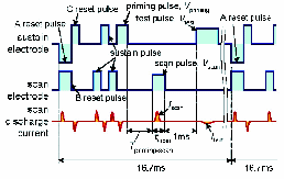
FIGURE 1 – Pulse waveforms for measuring discharge build-up and wall-charge-accumulation characteristics.
Recent research and development on 71-in.-diagonal color PDPs
Kwang-Yeol Choi
Jeong-Pil Choi
Myeong-Soo Chang
Eun-Ho Yoo
Won-Tae Kim
Jin-Young Kim
Eung-Chul Park
Seung-Tea Park
Jae-Hwa Ryu
Abstract — The first 71- and 76-in.-diagonal ACPDPs with full high-definition resolution (1920 x 1080), a high luminance of 800 cd/m2, and a dark-room contrast ratio of 1200:1 have been developed using a highly efficient barrier-rib structure. Also, a new MgO protective layer and a film-type optical filter were developed to improve picture quality. To fabricate large-sized panels over 70 in. on the diagonal, an improved uniform exposing technology for the patterning of electrodes, a green sheet method for the transparent dielectric layer, and a co-processed bus and black-matrix (CPBB) method were used.
Keywords — Full high-definition resolution PDP, barrier rib, co-processed bus and black-matrix method.
To achieve large-sized PDPs with diagonals of more than 70 in. with full HD resolution, several technical obstacles must be overcome. The panel area, which is more than 50% larger than that of 60-in. PDPs, requires improvements in the UV-exposing method, screen prints, and green-sheet laminating in order to achieve good panel uniformity. The number of total scan lines for HD-resolution PDPs should be increased by 40% more than that of XGA PDPs. The scan pulse width should be reduced and high-speed addressing is required. An increased number of data lines also requires high-speed signal processing. Large-area-panel fabrication technologies need to be developed for large-sized PDPs over 70 in. on the diagonal, and multi-panel processing makes it possible to achieve high throughput. For high picture quality, a full high-definition resolution of 1920 x 1080 is required.
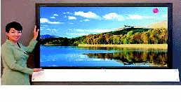
FIGURE 8 — LGE's 76-in. plasma-display panel with 1920 x 1080 pixels.
High-performance 55-in. diagonal WXGA PDP with extended ALIS technology
H. Kuriyama
M. Takeuchi
Y. Chiaki
K. Ohira
T. Shiizaki
Abstract — A high-performance 55-in.-diagonal WXGA PDP module with a novel structure by using Extended ALIS (Alternate Lighting of Surfaces) technology has been developed. The new cell structure that uses the common bus electrode concept was invented with a new driving scheme aimed toward progressive lighting. A new method of reducing dynamic false contour (DFC), motion adaptive subfield coding, was also developed. The newly developed 55-in. WXGA panel has a 1000-cd/m2 peak luminance and a 160-cd/m2full-screen white luminance with a 9000 K color temperature at a 350-W display power consumption.
Keywords — e-ALIS technology, progressive, motion adaptive, common bus electrode, phase-shifted sustain drive.
Based on ALIS technology, a new cell structure has been developed refered to as Extended ALIS (e-ALIS) for a WXGA panel with 768 x 1366 pixels. The front substrate has common bus electrodes, each of which is connected to transparent electrodes for two neighboring cells. Therefore, the total number of bus electrodes is 768 + 1, which is about half of 768 x 2 in a conventional WXGA panel. The transparent electrodes are ladder shaped for stabilizing discharge voltage. The box-type barrier-rib structure on the rear substrate enables a progressive lighting scheme with common bus electrodes, and also increases the aperture ratio and phosphor area. The aperture ratio of the new structure is 57%, which is about 1.4 times larger than that of the conventional structure. This high aperture ratio increases the luminance and luminous efficiency of the panel. The small number of bus electrodes, which is about half of that in a conventional panel, enables easy production with conventional fabrication design, and also enables the reduction of circuit cost.
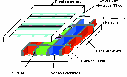
FIGURE 1 — Cell structure of e-ALIS panel.
Study of the effect of water on thermal and operating degradation of BaMgAl10O17:Eu2+ (BAM) blue phosphor
T. Onimaru
S. Fukuta
T. Misawa
K. Sakita
K. Betsui
Abstract — From the adsorption and desorption characteristics of water, it was shown that water can intercalate into BaMgAl10O17:Eu2+ blue phosphor. ESR, XANES, and XPS analyses confirmed that oxidation by water causes thermal degradation of BAM. It was also demonstrated that intercalated water accelerates luminance degradation under VUV irradiation and showed oxidation of Eu2+ during panel operation by means of μ-XPS. It was concluded that the cause of thermal and operating degradation of BAM is the oxidation of Eu2+ due to water.
Keywords — BaMgAl10O17, BAM, europium, intercalation, degradation, thermal, operating oxidation.
BaMgAl10O17:Eu2+ (BAM), a blue phosphor used in plasma-display panels (PDPs), has excellent characteristics for PDPs, in terms of luminance, color purity, after-image, etc. The crystal structure of BAM is a type of b-alumina, which is a typical layered material. A wide interlayer space, which a europium ion substitutionally occupies the barium sites, exists between the spinel layers. These interlayers are about 3 Å wide and allow molecules and ions to intercalate easily. Their intercalation has been the subject of intense investigation because β- and β²-alumina are promising materials for solid electrolytes and phosphors. The luminance of BAM degrades more than that of any other phosphor used in PDPs. It is necessary to overcome this problem. There are two types of BAM degradation. One is thermal degradation and the other is operating degradation.
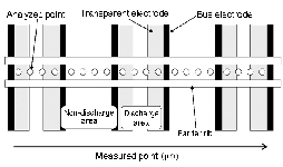
FIGURE 11 — Points measured along a barrier rib by μ-XPS.
Bit-depth extension: Overcoming LCD-driver limitations by using models of the equivalent input noise of the visual system
Scott Daly
Xiaofan Feng
Abstract — Continuous tone, or "contone," imagery usually has 24 bits/pixel as a minimum, with 8 bits each for the three primaries in typical displays. However, lower-cost displays constrain this number because of various system limitations. Conversely, higher-quality displays seek to achieve 9–10 bits/pixel/color, though there may be system bottlenecks limited to 8. This paper will report on techniques and observations made in achieving contone quality on ~100-or-less-ppi LCDs starting from 4- to 8-bit driver limits, and resulting with no visible dither patterns, noise, contours, or loss of amplitude detail at viewing distances as close as the near focus limit (~120 mm).
Keywords — Bit depth, dithering, visual models, spatiotemporal, displays, LCDs.
The general principle is that noise with a variance as high as possible without being visible to the user must be added. Since the average of a collection of numbers has a higher precision than the numbers themselves, the noise acts to increase bit depth because there is a subsequent averaging step that occurs in the optics of the display and the visual system. If the noise has a Gaussian probability density function (pdf), then the variance of the noise determines the resulting bit-depth extension. This holds whether the noise is white, high-pass filtered (HPF), or low-pass filtered (LPF); that is, the amount of contouring reduction is the same, regardless of spectrum.
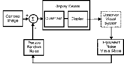
FIGURE 7 — Using only the visual model noise as "receiver" noise.
Plotting the course of the next VESA flat-panel-display measurements standard
Edward F. Kelley
Abstract — The Display Metrology Task Group of the Video Electronics Standards Association is developing the next Flat Panel Display Measurements Standard. The document's philosophy and the standard's acceptance will be reviewed. New directions will be reviewed, including more diagnostics, synthetic-face patterns, robust reflection measurements and their scaling, motion artifacts, and robustness of the measurement method.
Keywords — Display measurements, display metrology, display reflection, display standards, FPDM, synthetic faces, VESA.
In general, the aim of the Flat Panel Display Measurements Standard (FPDM) is to provide a metrology foundation for specification language and display characterization. Manufacturers who make quality displays should be able to brag about them using a bedrock foundation of good measurement methods. Those who use displays should be able to clearly specify the performance they need and then be able to measure the performance with agreed-upon methods of measurement. There is, therefore, a dual goal of defining the measurement method with a unique name and providing for robust and reproducible methods.
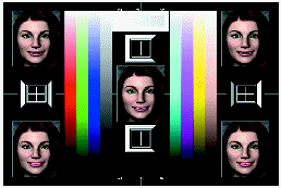
FIGURE 5 — Center and corner facial images with color bars and gray scale. F01-13 is provided as an example. The pattern is generated for each face. File nomenclature for this pattern is FaceCS13_hhhh x vvvv.png.
Measurement and evaluation of display scattering
Michael E. Becker
Abstract — A novel approach is introduced for the simple and effective measurement and evaluation of light scattering in general, and its application to electronic displays will be described. The method is based on the measurement of the lateral distribution of reflected luminance with an imaging detector. After numerical transformation of the measured luminance distribution, we obtained the characteristics of the BRDF of the sample with high directional resolution within a limited range of inclination angles centered about the specular direction. The method is easy to implement and to carry out. Due to the absence of moving parts, it exhibits only little sensitivity with respect to variations of the geometry parameters and is thus very robust. This paper summarizes the basics of the approach, establishes the relation to conventional BRDF-measuring methods, introduces an implementation and presents some typical results for LCD monitors.
Keywords — Display reflectance, glare, scattering, BRDF, PSF, ergonomic performance evaluation.
Since the first proposals to apply the method of the bidirectional reflectance distribution function (BRDF) to characterization of light scattering from visual displays, only a limited number of BRDF results obtained from commercial displays (e.g., LCD monitors) have been published. Measurement and evaluation of BRDF data still requires either a mechanical system for motorized scanning of the range of viewing directions (or source directions alternatively) or a conoscopic system that projects a collimated beam of light through its front lens on the sample while catching all of the rays reflected from the spot of the measurement. To provide the specular reflectance data over the required range with sufficient accuracy and robustness in combination with the detailed characteristics of high-resolution BRDF data without mechanical scanning, the following measurement approach was introduced: (1) application of an imaging photometer instead of a spot-photometer, (2) use of a high-intensity small-area source instead of a variable aperture source with integrating spheres, (3) numerical data processing to obtain the BRDF, and (4) numerical integration over the receiver aperture to obtain the specular reflectance factors rS1 and rS15 (ISO-13406-2).
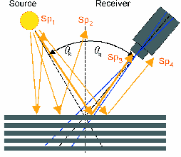
FIGURE 12 — Specularly reflected beams Sp1...Sp4 from different locations on the sample surface. Sp3 is received by the receiver with a non-specular inclination θR > θS.