Display Fabrication under Siege
The demand for high resolution, enhanced color depth, and faster switching speeds is challenging the STN-LCD and a-Si fabrication technologies used to make today's mobile displays. Where do they go from here?
by Marcel Führen
NEW, DEMANDING APPLICATIONS for the display systems designed into cellular telephones and other handheld electronic devices are pushing the limits of today's mainstream fabrication technology. Process engineers have successfully met many challenges in the past, but it is hard to remember any that were quite as daunting as those that now face them.
The primary drivers of mobile-display technology in the rapidly developing multi-media segment are imaging, video, and gaming. They are demanding drivers and are producing ambitious goals for the top-of-the-line displays of the not-too-distant future.
These goals include 24-bit color (16 million colors) and VGA resolution on a screen measuring less than 2.8 in. on the diagonal, a contrast ratio of more than 250:1, a luminance of more than 250 cd/m2, an NTSC ratio of more than 70%, an ultra-wide viewing angle, switching speeds less than 20 msec, and low power consumption. And the manufacturing technology that produces these highly capable displays must, of course, be both cost-effective and environmentally friendly.
Today's mainstream mobile-display technology is passive-matrix supertwisted-nematic (STN) technology, which encompasses both monochrome STN (MSTN) and color STN (CSTN) technology. The high resolution, color depth, front-of-screen performance, and switching speed required for multimedia segments mandate a migration to active-matrix thin-film-transistor (TFT) liquid-crystal-display (LCD) technology because it allows each pixel to be switched independently. But the challenges do not end there.
 Philips Mobile Display Systems
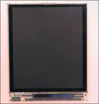
Fig. 1: In this typical small display, chip-on-glass (COG) display-driver ICs are mounted directly onto the display glass shown at the bottom of the photo.
The Limitations of COG
Typically, the control and driving electronics for small mobile displays are located in one or two integrated circuits (ICs) that are attached to the display glass using chip-on-glass (COG) technology (Fig. 1). COG was introduced in the '90s to reduce cost and minimize module size by attaching each driver-IC die directly to the display glass rather than using a separate circuit board or flexfoil. For COG, each pad on a driver-IC die is patterned with a gold interconnection bump that creates a coplanar, conductive path from the driver die to the glass surface.
For multimedia and video applications, COG has the advantage of employing standard silicon circuits that can switch at very high speeds. A drawback is that when a COG IC is mounted on the periphery of the display glass, it pushes the display window off center, which limits a product designer's flexibility to mount the display in the center of a product or freely position user-interface controls.
Another issue is that the number of connections to be made between the ICs and the glass surface for high-resolution displays can easily run over 1000, which diminishes yield and reliability. So, from the perspective of cost-effective manufacturing, it is desirable to integrate as much of the driving and control circuitry on the panel using the same semiconductor process as used for the pixel TFT switches. A large percentage of the technological innovation required to do this has already been developed.
Technology Contenders
There are two main contenders for active-matrix TFT technology: amorphous-silicon (a-Si) and low-temperature polycrystalline-silicon (LTPS) technology.
Compared to passive-matrix technology, a-Si active-matrix technology takes a big step forward by integrating in-pixel switching circuitry directly on the glass substrate of the panel. It greatly improves front-of-screen performance compared to that of passive-matrix STN technology. But one limitation of a-Si technology is that it lacks a monocrystalline structure. It therefore has low charge-carrier mobility, which, among other things, causes the TFT transistors to have poor stability – they cannot handle high-frequency signals.
Although innovative design work at several companies have made it possible to realize gate drivers that switch each line to operate each display pixel, there is no clear way to handle the logic and mixed-signal functions necessary for the source (column) drivers. Today, a-Si is used in about one-third of all new cellular-telephone displays. It offers pixel densities up to 250 pixels per inch (ppi).
LTPS was created by exposing a-Si to an intense laser beam that creates many small crystalline (polycrystalline) silicon structures on the glass. The charge-carrier mobility of polycrystalline silicon (poly-Si) is about 10% of that of the silicon used in IC manufacturing. This improved mobility, together with a higher TFT stability, permits the fabrication of CMOS transistors and enables analog, digital, and mixed-signal circuit designs to be applied to poly-Si structures on the display glass.
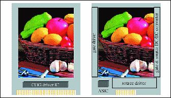
The elimination of the driver IC – or even the enabling of smaller or less complex ICs – creates a significant cost advantage, even though the costs of the LTPS panel are higher than those of a comparable a-Si panel (Fig. 2). The higher mobility of LTPS compared to a-Si results in a smaller "in-pixel" TFT, which gives LTPS a better front-of-screen performance for transmissive and transflective applications, especially at pixel densities greater than 250 ppi. This is because an in-pixel TFT does not transmit light, so a larger TFT reduces the aperture ratio – the percentage of pixel area that allows the light transmitted from the backlight to pass through the display.
Levels of Integration
Virtually all of the circuits required to operate a TFT-LCD could be fabricated directly on the glass substrate using LTPS technology. But a-Si technology can be tweaked to implement some of the driving electronics on the glass, thus resulting in lower cost.
The industry arrived at the first level of a-Si integration in 2004 when Philips Mobile Display Systems demonstrated reliable integration of gate-driver functionality in a-Si on glass. This development yields several positive results. It allows for a more symmetrical design, opens additional viewing area in the display, and paves the way for high pixel densities and more-cost-efficient a-Si TFT-LCDs.
The vital statistics of this 2004 module are a diagonal of 1.9 in., a QVGA resolution (240 x 320 pixels), and a color palette of 256,000 colors. The equivalent pixel density is 210 ppi.
 Philips Mobile Display Systems
Fig. 2: Shown is a rendering of a conventional small LCD panel with a COG driver IC and parallel interface (left) compared to an LTPS panel with on-panel integrated drivers and an ASIC for parallel to high-speed serial interface conversion (right).
To achieve higher levels of on-glass integration, the industry will almost certainly have to move on to LTPS technology. There are many other candidates for on-glass integration, including digital-to-analog converters, level shifters, multiplexers, dc-to-dc converters, and even memory.
Each circuit brings something new to the integration. On-glass integration of the dc-to-dc converter and capacitor for the gate driving voltage is important because it results in the display requiring only a single 3-V power supply because 3 V is already used to supply the logic circuits. But integrating the dc-to-dc converter for the digital-to-analog converter and common voltage is more challenging in view of the higher currents involved.
Memory integration promises similar advantages. The integration of a full-frame buffer would not be cost-effective or practical, but it is possible to integrate a partial frame buffer by integrating one or more bits of memory inside each pixel – an architecture referred to as memory in pixel (MIP) – which could provide a very low-power standby mode. When a static image, such as the one displayed while a cellular phone is in stand-by mode, is displayed, the use of MIP would permit the display and multiplexing circuits to be turned off, resulting in significant power savings.
A 1-bit memory cell behind each pixel provides eight-color capability. A prototype developed by Philips MDS in 2001 features a 384-column (128 x RGB) by 160-row TFT display that integrates a 1-bit/pixel frame-store memory and 4-bit DACs. Static images can be displayed in eight colors with a total power consumption of 1 mW. A more recent prototype shown at SID 2004 demonstrated MIP at 100 μW. And there is more to come.
But integrating memory circuits into the pixel has a negative effect on the aperture ratio, especially for transmissive applications. This is simply because light cannot pass through the circuit elements. One approach is to accept a lower aperture ratio as inevitable and to compensate by intensifying the backlight. Of course, this approach raises power-dissipation concerns. For transflective applications, Philips MDS showed in their 2004 demonstrations that even with a 1-bit MIP a transmissive/reflective ratio of 40:60 could be achieved.
Limits on Integration
Theoretically, it is possible to integrate most, if not all, of the logic onto the display glass. But there are a number of limiting factors, including yield, panel area, and data rates.
Higher levels of integration require more-advanced finer-design-rule LTPS processes, which will initially have lower yields than previous generations. Higher levels of integration also cause the peripheral electronic circuits to consume a larger area. These circuits have to fit along the 1.5–2.0-mm edges of the panel and on the COG area. If they do not fit, a more-advanced finer-design-rule process and/or breakthroughs in electronic circuit design are required.
The ability to buffer and process data at video speeds is also having an impact, particularly on the location and speed of memory circuits within cellular-telephone handsets. For example, a QVGA display capable of handling 24-bit color and 30 frames per second must operate with 100-Mbits/sec data rates; moving on to VGA resolution would require handling data rates greater than 400 Mbits/sec.
There is also a trend in these high-resolution displays to move the frame buffer from the display module to the baseband system, thus requiring the LCD to be refreshed at 60–70 Hz over the display-module interface. Partitioning the system in this way requires more than 24 wires running in parallel over flexfoils in the module using standard CMOS signaling levels.
This presents electro-magnetic interference (EMI) problems at the high data rates needed for QVGA and higher-resolution displays. It is to be expected that over time the industry will abandon parallel interfaces and use serial communication based on low-voltage differential signaling (LVDS), which has the benefit of lower EMI and will result in further miniaturization (Fig. 3). Standardization in this area is currently moving forward in the Mobile Industry Processor Interface (MIPI) consortium.
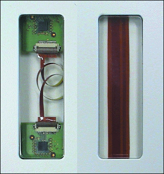
Fig. 3: Serial flexfoil used with a high-speed serialized display interface (left) requires fewer conductors and occupies less volume than a conventional parallel RGB interface (right).
But even the higher carrier-charge mobility of LTPS will likely not be high enough to support the required transmission speeds of more than 100 MHz. A serial-to-parallel converter IC, to be mounted via COG or chip-on-foil (COF) technology, will be required.
As is always the case with display-fabrication technology, there is no simple answer. Successful products are those that find the most advantageous combination of engineering tradeoffs between the benefits and costs of each technology. This is one reason that COG technology, for example, will remain part of mobile displays for quite some time. As the level of integration increases, LTPS will gradually gain market share over a-Si, starting with high-end displays and migrating to the more plebeian market segments.
Conclusion
Displaying video and multimedia content on cellular telephones and other mobile devices will push the display-fabrication industry to accelerate the development of new technologies, including a-Si, LTPS, and advanced backlighting.
Although CSTN is not capable of addressing high-resolution segments of the market, it will remain an important technology for entry-level segments for at least the next few years. Amorphous silicon will grow in popularity, rising from its current 30% volume market share. LTPS offers unprecedented opportunities to integrate logic on glass.
Although LTPS represents only 12.2% of the market in 2005, it is likely to grow to 30% – which represents the high-end segment – in the next few years, according to DisplaySearch's Quarterly Mobile Phone Shipment and Forecast Q3 '05. COG will remain the dominant technology for integrating a driver or controller IC in a display module, and the industry's overall strategy will be to find the best combinations of technologies that work best for specific market segments. •
Marcel Führen is Senior Director of Advanced Technology at Philips Mobile Display Systems, Bldg. W-122, Jan Campertstraat 5, 6416 SG Heerlen, The Netherlands; telephone +31-45-5437-791, e-mail: marcel. fuhren@philips.com.