A preview of the papers appearing in the August 2006 issue of the Journal of the SID. To obtain access to these articles on-line, please go to www.sid.org
Edited by Aris Silzars
Voltage-programming method with transimpedance-feedback technique for threshold voltage and mobility compensations in large-area high-resolution AMOLED displays
Hai-Jung In
Pyong-Su Kwag
Jin-Sung Kang
Oh-Kyong Kwon
Ho-Kyoon Chung
Hanyang University, Korea
Abstract — A voltage-programming method using a transimpedance-feedback control technique is proposed for compensating threshold voltage and mobility variations of driving thin-film transistors (TFTs) in large-area high-resolution polycrystalline-silicon (poly-Si) active-matrix organic light-emitting-diode (AMOLED) displays. Those electrical characteristic variations of TFTs throughout a large-area high-resolution panel result in picture-quality non-uniformity of AMOLED displays. The simulation and experimental results of the proposed method show that the maximum emission-current error for 30-in. full-high-definition television (HDTV) applications is less than 1.9% when the mobility variation and the threshold-voltage variation are ±12.5% and ±0.3 V, respectively. The proposed method is the best programming method for large-area high-resolution AMOLEDs among the published methods.
Figure 1 shows a schematic diagram of the proposed driving and pixel circuits. Driving circuits are constructed with single-crystalline metal-oxide-silicon (MOS) transistors, and pixel circuits are composed of poly-Si TFTs on an LTPS panel. The P1 TFT is used as the driving TFT of the pixel, so the emission current, which is generated from the P1, strongly depends on the electrical characteristics of the P1 TFT. The driving sequence consists of threshold-voltage-compensation, pre-charging, voltage-sensing, voltage-programming, and emission phases.
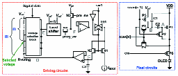
FIGURE 1 — The proposed driving schematic diagram and pixel circuits.
Properties of column spacers on a flexible color filter using a roll-to-roll process
A. Sonehara
T. Eguchi
A. Sugizaki
A. Kumano
T. Ito
T. Takahashi
Technology Research Association forAdvanced Display Materials (TRADIM),Japan
Abstract — Column spacers were manufactured by a roll-to-roll process for a flexible plastic substrate and an LCD prototype was demonstrated for the first time. The purpose of this paper is to obtain a stable cell gap for plastic LCDs by designing the column spacers. The optimum condition was derived for the properties of the column spacers parameters, such as the cross section, density, and hardness. As a result, the optimum elastic modulus of the column spacers needed in order to precisely maintain the cell gap of the LCD as well as that of conventional glass plates could be determined, resulting in a uniform display luminance.
In the case of a flexible plastic substrate, the transfer method (FMT method) was found to be one of the best ways to create column spacers. The reasons are (1) the transfer method excels at web handling to simplify manufacturing equipment. (2) It can produce a uniform height for the column spacers despite the surface roughness of the substrate film because a uniform thickness of the layer for column spacers is conformably transferred. (3) Exposure through the cover film can make the photopolymer sensitive to oxygen inhibition and also can decrease the amount of initiator in the polymer. (4) Exposure through the cover film can prevent particles from attaching to the surface of the column-spacer layer during exposure.
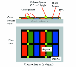
FIGURE 4 — Layout design of column spacers on a color filter.
What is needed in LCD panels to achieve CRT-like motion portrayal?
A. A. S. Sluyterman
Philips Lighting, The Netherlands
Abstract — In LCD panels, motion portrayal as well as panel-addressing speed and response time are critical. They need to be balanced carefully, in particular for HDTV. It will be shown which combination of technologies, such as response-time improvement, black-frame insertion, double frame rate, and scanning backlight, can achieve CRT-like motion portrayal without demanding extreme response speeds from the panel.
The "hold effect" in an LCD can be reduced via its backlight. By illuminating each area on the screen only for a short period of time, the "hold effect" is reduced and motion fidelity is improved. A scanning backlight (see Fig. 7) is a direct-lit backlight, in which the illumination timing of each of the light sources varies from top to bottom according to the writing of video content into the panel. In a practical scanning backlight, however, the luminance profile will not look exactly like a block. This is caused by the fact that, for reasons of overall luminance uniformity, there must be some overlap of the regions on the screen that are illuminated by the successive light sources. This is called optical crosstalk. It is, in fact, the combination of the optical crosstalk and the difference in illumination timing between the successive light sources that causes this broadening of the luminance profile on the screen.
FIGURE 7 — A scanning backlight is a direct-lit backlight, in which the light sources emit light only for a short fraction of the frame-period time, and in which the light sources are ignited one after the other.
An intensively lit collimating unit for the realization of a mosaic-structured large-scale RGB backlight
Kälil Käläntär
Nippon Leiz Corp., Japan
Abstract — To realize a large-scale LCD backlight, a hexagon-shaped single-side micro-structured light guide was developed. Three of the micro-structured light-guide plates are stacked and combined with a circular prism sheet (CPS) to form a unit backlight. The light guides couple azimuth light radiation from a side-emitting LED that is mounted at the center of the light guides to air through a CPS in order to make a plane source out of a point source. The combination of stacked functional light guides with a CPS transforms convex toroidal-shaped light radiation into a narrow cone whose center axis is perpendicular to the back surface of the liquid-crystal panel. The light efficiency of the illumination unit is about 78% and the full-width at half maximum of the collimated light is about 2 and 32.5° in the azimuth and radial directions, respectively.
An array of spatially distributed unit backlights (UBLs) is a solution to realize a large-scale backlight. The unit backlight uses stacked functional light-guide plates (LGPs). These light guides are combined with a side-emitting LED that has an azimuth radiation pattern and a circular prism film (CPS). A stack of thin light guides is applied to the UBL to increase the light-extraction efficiency. Each light guide has an array of concave micro-reflectors (MRs) on the rear side that reflects and directs the guided light toward the front surface.
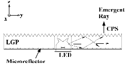
FIGURE 4 — A cross section of the UBL. The light tracing and the light extraction are shown in the backlight.
Development of a 25-in. SVGA SMPDP
Qing Li
Xiong Zhang
Yongming Tang
Yan Tu
Zhaowen Fan
Lanlan Yang
Yaosheng Zheng
Baoping Wang
Southeast University, P. R. China
Abstract — A newly developed 25-in. SVGA ACPDP containing a shadow mask (SMPDP) is presented. Some modifications have been introduced into the fabrication technique. Instead of using conventional Ag in a thick-film process, an aluminum bus electrode without ITO was fabricated on the front substrate, which was made by using a thin-film process. Due to this improvement, excellent uniformity of the dielectric layer has been achieved. Only five necessary process steps are required during the manufacturing process of the front/rear substrates for the SMPDP. The panel capacitance was reduced by over 20% by adopting an ITO-less structure, which enables high-speed addressing for large-capacity displays. The color purity was improved by applying a high Xe content.
The structure of an SMPDP is shown in Fig. 1. The front and rear substrates are almost identical to that of a conventional coplanar-structured PDP. To reduce the capacitance and fabrication costs, parallel scan electrodes without ITO are applied to the front glass substrate. Address electrodes, placed orthogonally to the scan electrodes, are applied to the rear substrate. A dielectric layer is formed on these electrodes and a MgO protecting layer is evaporated on the dielectric layer. Tri-primary color phosphors (red, green, and blue) are formed on the inner surfaces of the shadow-mask cell.
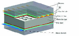
FIGURE 1 — Panel structure of the SMPDP.
Front address structure for high luminous efficacy and low address voltage in ACPDPs
Masaki Yoshinari
Yoichi Shintani
Tasuku Ishibashi
Yoichi Okumura
Toshihiro Komaki
Pioneer Corp., Japan
Abstract — 8-in. AC plasma-display panels with front address (FA) structures were developed. Deep barrier ribs, high-Xe-content gas, and long sustain gaps were applied to FA structures to achieve high luminous efficacy. The FA structures have several advantages over conventional structures. Because address electrodes are closer to sustain electrodes, FA PDPs can be driven at lower address voltages, under the condition of deep barrier ribs or high-Xe-content gas, than conventional PDPs. A disadvantage of FA PDPs is relatively high capacitance between the sustain electrodes and address electrodes compared to that of conventional PDPs.
In this FA structure, because sustain electrodes and address electrodes are placed in the same front glass plate, the distance between the sustain electrodes for scan and address electrodes is shorter than that in conventional PDPs. In FA structures, address voltages are lower than those of conventional PDPs at deep barrier ribs and high Xe content. It seems that barrier-rib height and phosphors do not affect address voltages. Figure 9 shows the schematic structure of FA PDPs with low capacitance. As shown in Fig. 9, the second dielectric layer is located on the first dielectric layer. Address electrodes are located on the second dielectric layer and covered with the third dielectric layer.
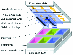
FIGURE 9 — Schematic structure of front-address PDPs with low capacitance.
Feasibility of driving PDPs with 1-V data and 30-V scan pulses by controlling the self-erase-discharge threshold
A. Saito
T. Shiga
S. Mikoshiba
The University of Electro-Communications, Japan
Abstract — In order to realize low-voltage addressing of PDPs, an erase-addressing scheme was adopted together with an accumulation of an appropriate amount of wall charge by using priming and bias pulses prior to addressing. The switching operation is performed by using sharp threshold characteristics of the self-erase discharge. Cessation of the scan pulse ignites a weak self-erase discharge, which, together with the data pulse, triggers an intense self-erase discharge. By using the drive scheme, the data- and scan-pulse voltages can be reduced to 1.1 and 29.6 V, respectively, provided that the panel has perfectly uniform voltage characteristics.
Erase-address waveforms utilizing the self-erase-discharge threshold are shown in Fig. 6. The proposed addressing scheme is as follows. Prior to addressing, the priming pulse discharge with V
priming 0 = 214 V is generated. Then the wall charge corresponding to V
wall = 214 V are accumulated at
t1. This value is slightly smaller than the threshold of the self-erase discharge, namely, slightly at the left of the border of regions (2) and (3). At the end of the priming pulse,
t2, the scan electrode voltage is dropped to V
scan = 30 V by the amount V
priming = 184 V. The magnitude of V
scan is made equal to the width of region (2). When the priming-pulse voltage drops from V
priming 0 to V
scan by the amount V
priming, there is no discharge, and the wall-charge accumulated by the priming pulse is preserved. When the scan voltage drops to 0 at
t3, a weak self-erase discharge is ignited between the data and scan electrodes.
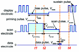
FIGURE 6 — Erase-address pulse voltage waveforms utilizing the self-erase-discharge threshold.
2-D/3-D switchable displays
O. H. Willemsen
S. T. De Zwart
M. G. H. Hiddink
O. Willemsen
Philips Research Laboratories, The Netherlands
Abstract — In this paper, the design of a lenticular-based 2-D/3-D display for mobile applications is described. This display combines look-around capability with good 3-D resolution. In order to allow high-resolution datagraphic applications, a concept based on actively switched lenses has been developed. A very noticeable problem for such displays is the occurrence of dark bands. Despite slanting the lenticular and defocusing the lens, banding becomes unacceptable when the display is viewed from an angle. As a solution, fractional viewing systems to reduce the banding intensity by almost two orders of magnitude is introduced. The resulting 3-D display can be viewed from any horizontal direction without banding.
Figure 5 shows the basic principle of the active LC filled lens. It consists of two plates coated with indium tin oxide (ITO) to serve as electrodes. On the first plate, a negative fixed lens structure is replicated using photo-polymerization. The high-index axis of the LC is aligned in the direction perpendicular to the plane of the drawing if no voltage is applied over the cell. If the light from the underlying LCD is polarized perpendicularly to the plane of the drawing, it encounters a high refractive index within the LC, resulting in a net lens action. If a voltage is applied over the cell, the axis of the LC is aligned parallel to the lens axis, in the plane of the drawing. Since the ordinary refractive index matches the refractive index of the replica layer, the lens is effectively switched off. This causes the native resolution of the underlying display to be regained.
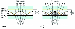
FIGURE 5 — Principle of an actively switched lenticular lens in (a) the 3-D mode and (b) the 2-D mode.
Hollow fibers containing various display elements: A novel structure for electronic paper
Masahiro Nakata
Masahide Sato
Yoshinori Matsuo
Shuichi Maeda
Shigeo Hayashi
Oji Paper Co., Ltd., Japan
Abstract — A novel structure for electronic-paper displays using hollow fibers has been developed, where the hollow fiber is comprised of an outer transparent polymer tube and inner display elements (rotating balls, electrophoretic dispersion fluid, or cholesteric liquid crystals). The structure composed of thin polymer fibers is capable of realizing paper-like visibility and flexibility, which are vital properties required for electronic-paper displays. Hollow fibers containing display elements were produced through an industrial manufacturing process using a conventional melt spinning method for the first time and showed electro-optical switching when the voltage was applied. The hollow fibers were then woven into fabric sheets. The structure and the production process for electronic paper in this study will be a candidate for a simple method to produce large-area electronic-paper displays.
One of our motivations in focusing on hollow fibers is that the structure of woven fibers can give paper-like visibility. When a fabric sheet is made by weaving hollow fibers, a fiber display with a woven structure is obtained, as shown in Fig. 1. This woven structure of hollow fibers is considered to be similar to the tangled structure of cellulose fibers in paper. The readability of paper, which most electronic paper technologies are aiming at, is mainly attributable to the fact that paper scatters light in all directions irrespective of the angle of the incident light. The light scattering is caused by the tangled structure of the cellulose fibers. Therefore, this woven fiber display is thought of electronic paper with a "paper-mimetic" structure.
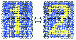
FIGURE 1 — Schematic diagram showing an electronic-paper display made of hollow fibers.
Flexible electronic-paper active-matrix displays
H. Edzer A. Huitema
Gerwin H. Gelinck
Pieter J. G. van Lieshout
Erik van Veenendaal
Fred J. Touwslager
Philips Technology Incubator,The Netherlands
Abstract — A 100-μm-thick 320 x 240-pixel active-matrix display integrated into a functional-device prototype is presented. The active matrix is composed of alternating layers of organic materials and gold. A six-mask photolithographic process is used. An electrophoretic electronic imaging film is laminated on top of the active matrix. The display is bendable to a radius of 7.5 mm for more than 30,000 repetitions.
The most exciting feature of rollable display devices is that the display area can be larger than the device area itself. This means that the rollable QVGA having a diagonal of 4.7 in. and a roll radius of 7.5 mm can be stored in a device that has a diagonal considerably smaller than 4.7 in. and a thickness that is close to 15 mm. For the QVGA display, integration into a device yields a display area that is more than 150% of the device area. When going to larger display sizes, this advantage becomes even larger.
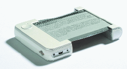
FIGURE 7 — Photograph of the functional Readius prototype in its rolled-out state. The display area is 110% of the device area.
A transparent sheet display by plastic MEMS
Yusuke Taii
Akio Higo
Hiroyuki Fujita
Hiroshi Toshiyoshi
University of Tokyo, Japan
Abstract — A new type of color-image display pixel based on MEMS (microelectromechanical systems) technology of plastic materials is presented. The mechanism for making color is optical interference using a Fabry-Perot interferometer. A thin sheet of PEN (polyethylene naphthalate) with a metal half-mirror was laminated over a glass or PEN substrate with an optical cavity inside. The electrostatically controlled deformation of the PEN film changes the color of the transmitting light by interference within the optical cavity. Color pixels of three primary colors (red, green, and blue) were successfully developed and demonstrated, with a driving voltage ranging from 80 to 120 Vdc . Thanks to the mechanical flexibility of the PEN films, the display could operate even when placed on a curved surface.
Figure 3 shows the OFF and ON states of the membrane in operation: the top-view color images were taken with an optical microscope with a color CCD camera, and the transmission spectrum was obtained by numerical simulation. When no voltage was applied, the PEN membrane was at the flat rest position, and the transmitted light appeared dark gray to the viewer's eyes due to the superposition of several transmission peaks, as shown in Fig. 3(a). When the voltage was applied between two aluminum layers, on the other hand, the upper film was electrostatically pulled into contact with the bottom substrate to squeeze the air gap, resulting in a change in the transmission color. The transmitted light interferes only in the silicon oxide layer, which produced a green color as shown in Fig. 3(b).
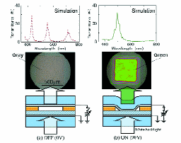
FIGURE 3 — Schematic illustration of the OFF and ON states of the deformable membrane. (a) Gray color with a suspended membrane with no bias and (b) green color in electrostatic pull-in at 90 Vdc.