A preview of the papers appearing in the November 2005 issue of theJournal of the SID, available on-line at www.SID.org.
Edited by Aris Silzars
A high-luminous-efficacy PDP having multi-anodes for reduction of ionic effect (MARI)
Jeong-Doo Yi
Joon-Yeon Kim
Tae- Woo Ki m
Hak-Cheol Yang
Jeong-Nam Kim
Yoon-Hyoung Cho
Samsung SDI
Abstract — A PDP having a new structure and driving scheme is proposed. An auxiliary electrode was inserted between X and Y electrodes. Driving and discharge stability was determined using a test panel. A 42-in. SD (852 x 480) panel and a 42-in. HD (1366 x 768) panel were also made having this new structure, and the increase in luminous efficacy and the reduction of ionic losses were verified. A luminous efficacy of 2.35 lm/W in an SD panel and 1.97 lm/W in a HD panel were achieved. Finally, the characteristics and merits of the new structure were investigated.
The new PDP structure is shown in Fig. 1. The resulting cell structure is almost the same as that of a conventional three-electrode coplanar PDP structure. But there are differences between MARI and conventional PDPs. Between the X and Y electrodes, an auxiliary electrode was inserted. During the sustain period, electrons remain attached to the auxiliary electrode, so ionic heating losses are reduced. This new type of PDP is referred to as a multi-anode to reduce the ionic effect in MARI PDPs. A new driving scheme was developed. The auxiliary electrode is used as a reset and scan electrode. In a MARI PDP, the total electrode length does not change, but the electrode length of the anode is effectively increased with the auxiliary electrode in both sustain phases.
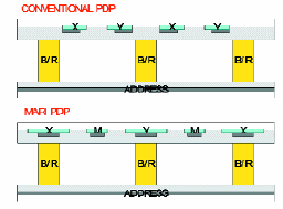
FIGURE 1 — Schematic diagram of a conventional PDP and a MARI PDP. The rear-plate structure is the same as that of a conventional PDP, but the front plate is different. An auxiliary electrode is inserted between the X and Y electrodes.
High-efficiency PDP micro-discharges
G. Oversluizen
T. Dekker
Philips Research Laboratories
Abstract — The interdependency of the capacitive design, the sustain voltage, and the Xe content will be discussed. A high panel efficacy was obtained, especially for the design and driving conditions that govern the development of a fast discharge. A fast discharge was observed for a higher discharge field at sustain voltages higher than 200 V. It is proposed that in this mode the cathode sheath is not, or incompletely, formed during the increase in the discharge current, and the electric field in the discharge cell is dominated not by the space charges but by the externally applied voltage. The effective discharge field is lowered, resulting in a lower effective electron temperature and more efficient Xe excitation. Also, under a fast discharge build-up condition, the electron-heating efficiency increases due to a decrease in the ion heating losses in the cathode sheath.
The discharge evolution was investigated for two cell designs; the default cell design and a +C-buffer design including a buffer capacitor. Figures 5(a)–5(c) show schematic cross-sectional views of the default front plate and the +C-buffer front plate, and the electrical circuit indicating the additional capacitance Cp for the case of the +C-buffer design. Stray capacitance is not considered in the simplified circuit. The Cp counterelectrodes were all interconnected at the panel edge. In this way, a capacitance parallel to the discharge was created. In our +C-buffer design, Cp/Cd is about 1, and Cd is 0.13 pF/color subpixel.
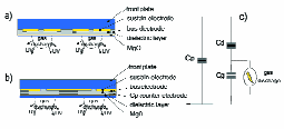
FIGURE 5 — Cross sections of the default and the adapted front-plate design that includes a buffer capacitance, and the corresponding electrical circuit.
DIA-PDP with high luminous efficacy and increased vertical resolution
Shinsuke Yura
Shigeki Harada
Ko Sano
Shinichiro Nagano
Mitsubishi Electric Corp.
Abstract — A PDP utilizing a new cell configuration to improve the vertical resolution and luminous efficacy is proposed. In this configuration, a delta subpixel arrangement is adopted because it reduces the vertical pixel pitch by half and increases the vertical resolution. In this configuration, R, G, B subpixels form triangles which are diamond shaped, the rational for calling this technology "DIA-PDP." High luminous efficacy is achieved by reducing the reflectivity of the panel. The lower reflectivity enables increased transmittivity of the light-reduction filter which is part of the PDP panel, thus ensuing sufficient contrast under bright conditions. The higher transmittivity increases the luminous efficacy with the filter. Results obtained for a 46-in. panel demonstrate a 33% increase in the luminous efficacy when using the filter. The DIA cell configuration is further modified to be a "clustered DIA" in order to improve the color mixing. Through subjective evaluation, the color mixing was compared with that of panels based on a trio subpixel arrangement and DIA, and the effect on color mixing was confirmed. The luminous efficacy of clustered DIA is also shown to be equal to that of DIA.
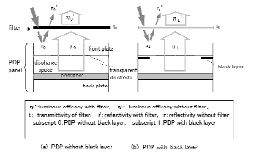
FIGURE 3 — PDP model that explains the improvement in luminous efficacy. (a) PDP without black layer, (b) PDP with black layer.
FIGURE 4 — Cell configuration of 46-in. DIA-PDP.
High-luminous-efficacy structure for plasma tubes
Manabu Ishimoto
Hitoshi Hirakawa
Kenji Awamoto
Koji Shinohe
Hitoshi Yamada
Yosuke Yamasaki
Tsutae Shinoda
Fujitsu Laboratories, Ltd.
Abstract — The plasma-tube-array display is expected to become a wall-sized display with very high luminous efficacy. The cell design for high luminous efficacy was investigated. Also, discharging in the plasma tube was observed in order to investigate the structure for high luminous efficacy. As a result, a high luminous efficacy of 5.4 lm/W was achieved.
The plasma tube has a wider design valuation than conventional PDPs. For example, a far wider sustain gap than conventional PDPs is possible. The tube design and its optimization for high luminous efficacy is described. The luminous efficacy is proportional to the sustain gap. Also, the efficacy increases by a large volume angle from the discharge to the phosphor layer. High-Xe-content discharge gas improves the efficacy the same as that for conventional PDPs.
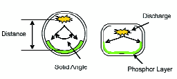
FIGURE 19 — Efficacy difference using a UV ray with different tube shapes.
High-speed low-voltage driving of high-Xe-content PDPs with priming particles
T. Shiga
A. Saito
M. Tone
S. Mikoshiba
G. Oversluizen
The University of Electro-Communications
Abstract — By examining PDPs having 3.5%–30% Xe content, it was found that utilization of the space-charge priming effect as well as wall-charge accumulation are effective in obtaining a low operating voltage and a high switching speed. The improvements are enhanced for higher Xe pressures. By using space-charge priming, the statistical time lag of the discharge triggering for the 30% Xe content is reduced significantly and becomes approximately equal to that of 3.5% Xe content. Once triggered, the formative time lag of the discharge becomes shorter and the space charge experiences diffusion/drift; hence, accumulation of the wall charge is faster for discharges with higher Xe contents. These indicate that the use of an erase addressing scheme, rather than a write addressing scheme, is preferable when driving high Xe-content PDPs, because the erase addressing scheme provides the addressing operation with an abundant amount of priming particles. Also, the drive voltages are lower for the erase addressing scheme. In order to reduce the address voltage, it is effective to accumulate wall charges prior to addressing. It was found that there are limiting values for the charge accumulation, above which self-erase discharges ignite and the wall charge is dissipated. The self-erase discharge occurs at relatively low wall voltages when the Xe percentages becomes higher. The sustain pulse voltage can be reduced while keeping the luminous efficiency high by increasing the sustain pulse frequency. As the frequency is increased, a residual amount of space charge created by the preceding sustain pulse increases. Due to the priming effect of these space charge, the build-up of the discharge current becomes faster, resulting in a lower voltage.
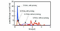
FIGURE 1 — Current waveforms of scan discharges between the scan and sustain electrodes with and without priming particles. The scan pulse is applied at time 0.
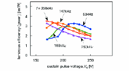
FIGURE 9 — Luminous efficiency (green) vs. sustain-pulse voltage, Vs, for values of sustain-pulse frequencies, f,10% Xe.
Address pulses during sustain period for increasing luminous efficiency
Heung-Sik Tae
Kyungpook National University
Abstract — A new driving method using a short pulse applied to the address electrode (i.e., address pulse) during a sustain period is proposed to improve the luminous efficiency. In this method, short pulses are additionally applied to the address electrode during the rising or falling edge of the sustain pulses. In the case of a small sustain gap, address pulses synchronized with a rising edge of the sustain pulse can help the expansion of the discharge volume toward the address electrode, whereas address pulses synchronized with a falling edge of the sustain pulse produce a self-erasing discharge, which improves the luminous efficiency. In the case of a large sustain gap, the application of the address pulse can produce a stable sustain discharge at a low sustain voltage level, generating an efficient discharge even in the case of the long discharge path.
It is important to investigate the changes in the discharge characteristics according to the relation between the sustain and address pulses. In addition, it is also important to examine the discharge characteristics, depending on the difference of the sustain gap when applying the address pulse together with the sustain pulse. Figures 1(a) and 1(b) show the schematic diagrams of the cell structure of an ACPDP with (a) a small sustain gap (60 μm) and (b) a large sustain gap (400 μm).
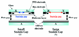
FIGURE 1 — Schematic diagram of ACPDP cell with (a) small and (b) large sustain gaps employed in this research.
Development of a new blue CaMgSi2O6:Eu2+ phosphor for PDPs
Takashi Kunimoto
Hiroshi Kobayashi
Ryo Yoshimatsu
Shingo Honda
Eisuke Hata
Shigeyasu Yamaguchi
Koutoku Ohmi
Tokushima Bunri University
Abstract — A blue-light-emitting Eu2+-doped CaMgSi2O6 phosphor having a long lifetime for a plasma-display panel (PDP) was developed. The CaMgSi2O6:Eu2+ (CMS:Eu) phosphors show no luminance degradation during the baking process, and an equivalent photoluminescence peak intensity compared to that of the conventional blue-phosphor BaMgAl10O17:Eu2+ (BAM) after baking. CMS:Eu shows a poor luminescent characteristic for the Xe excimer band excitation due to the lack of absorption. To introduce the absorption center for the Xe excimer band, Gd-codoping of CMS:Eu as a sensitizer was performed and a new excitation band around 172 nm was found, which originated from Gd3+. The test PDPs panels using synthesized CMS:Eu phosphor and CMS:Eu,Gd phosphor were examined to investigate the luminescent and aging characteristics of a Xe-discharge excitation source. The CMS:Eu panel shows an emission peak intensity comparable to that of the BAM panel (i.e., a comparable stimuli L/CIEy, 93% of BAM), while the CMS:Eu,Gd panel shows poorer blue emission intensity compared to the BAM panel (up to 53%of total stimuli of BAM). The CMS:Eu panel and the CMS:Eu,Gd panel show less luminance degradation than the BAM panel under the aging test, and the panel retains 90% of its luminance after 300 hours of driving. It was found that CMS:Eu appears to be a candidate for a new blue PDP phosphor because of its longevity in a Xe-discharge plasma environment.
The luminous efficiency and lifetime of PDPs are directly related to the performance of the phosphors used in PDPs. High-energy photons from the Xe discharge (147-nm resonant line, 8.4 eV, and 172-nm excimer band, 7.2 eV) are used as the excitation source of PDPs. Thus, a higher efficiency, a higher stability under high-temperature processes, and long lifetime under vacuum-UV (VUV) irradiation are major concerns in selecting suitable phosphors for PDPs. With regard to these requirements, current VUV phosphors have some disadvantages. In particular, BaMgAl10O17:Eu2+ (BAM), which is currently used as the blue PDP phosphor, shows serious luminance degradation during the heating processes for binder burn-off and by the plasma environment during operation.
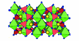
FIGURE 1 — The projection of CaMgSi2O6 on [100]. Red and Green polyhedra represent the SiO4 tetrahedra and MgO6 octahedra, respectively. Yellow and blue spheres represent the Ca and O ions, respectively.
Influence of barrier-rib morphologies on PDP efficacy
Tae-jung Chang
Do-Young Park
Ki-In Kim
Jin-Seok Kim
Yong-Seog Kim
Hongik University
Abstract — In this study, the effects of barrier-rib morphology on the luminance efficacy of PDPs were examined. Barrier ribs such as stripe, waffle, rectangular, honeycomb, SDR, and inverse SDR types were prepared using the capillary molding process. By using rear plates with such barrier ribs, the luminance and its efficacy were measured. The results demonstrated the feasibility of a capillary molding process in fabricating high-efficacy PDP discharge cells.
FIGURE 1 — Schematic illustration of (a) mold preparation and (b) capillary molding processes.
Implications of microcavity plasma devices for new plasma-display-panel cell structures with improved luminosity
S.-J. Park
K.-F. Chen
S.-H. Sung
C. J. Wagner
J. G. Eden
University of Illinois at Urbana-Champaign
Abstract — The unique properties of microcavity plasma devices, and their potential to provide the basis for alternative PDP cell structures of improved luminosity, are described. Arrays as large as 500 x 500 (250,000) inverted pyramid microcavity devices, each with an emitting aperture of 50 x 50 μm2 and designed for AC or bipolar excitation, have been fabricated in Si and operated in the rare gases and Ar/N2 mixtures at pressures up to and beyond 1 atm. For a device pitch of 100 μm, the array filling factor is 25% and the device packing density is 104 cm–2. Measurements of the unoptimized radiant output of 500 x 500 arrays of Si microplasma devices, operating in Ne/(5–50)% Xe mixtures and photoexciting (in transmission mode) a 20-μm-thick film of green phosphor, yield values of the luminous efficacy up to 7.2 ± 0.6 lm/W for a Ne/50% Xe mixture (total pressure of 800 Torr) excited by a 20-kHz sinusoidal voltage waveform. Sustaining voltages ranging from ~250 to 340 V (RMS) yield luminance values up to ~2000 cd/m2 for Ne/50% Xe mixtures, but the incorporation of field emitters or MgO into the microcavity is expected to significantly reduce the required operating voltage.
FIGURE 1 — Diagram (not to scale) of the cross section of an inverted square pyramid microcavity plasma device, fabricated in Si and designed for AC or bipolar waveform excitation. The dimensions of the pyramid at its base (i.e., emitting aperture of the microcavity) are 50 x 50 μm2 for the data presented here.
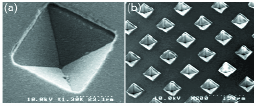
FIGURE 2 — Scanning electron micrographs (SEMs) of (a) a single inverted-pyramid microcavity plasma device with base dimensions (emitting aperture) of 50 x 50 μm2, and (b) a portion of an array of micro-plasma devices in which the device pitch is 100 μm.
Improvement in luminance, luminous efficiency, driving margin, and operational lifetime of HD PDPs by using discharge deactivation film
Shinichiro Nagano
Ko Sano
Takayoshi Nagai
Keisuke Jo
Seitaro Makino
Shinsuke Yura
Mitsubishi Electric Corp.
Abstract — A 116-cm HD PDP was improved in many respects by using DDF formed on MgO around the display line boundaries. The DDF allows an extremely narrow inter-pixel gap even for a stripe-rib structure because it prohibits vertical crosstalk discharge. The DDF combined with a stripe-rib structure results in the best address discharge response. Thus, a very wide driving margin area is achieved, allowing for a high percentage of Xe. The preferable sustain electrode shape follows the CAPABLE DDF style, where the principal discharge portion is separated from the bus via slim bridge. This cell configuration proved to be excellent in operational life testing with respect to DDF as well as in manufacturing process margin. By employing both a thinner dielectric layer and a TiO2reflective underlayer for phosphor, the address response is further improved so that Xe15%vol. is available from the viewpoint of the driving margin. Thus, we achieved a white peak luminance of 1220 cd/m2 and a luminous efficiency of 2.16 lm/W simultaneously despite an applied sustain voltage as low as 185 V; they will soon be as high as 1400 cd/m2 and 2.5 lm/W by modifying the sustain electrode style.
The DDF should be formed of insulating material such as Al2O3, TiO2, or SiO2, which has a far lower secondary electron emission coefficient (γi) than MgO. This prevents gas discharges from taking place on the DDF surface despite the bus electrodes underneath. Therefore, by properly setting the DDF width, the gas discharge in each display line is spatially isolated enough to prevent vertical crosstalk discharges. This encourages the use of a stripe-rib structure, which is more advantageous than a box-rib structure in many aspects for HD (high definition) PDPs.
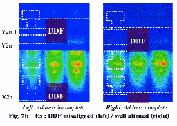
FIGURE 7 — ICCD images of address discharge in samples F and Es.
Discharge efficiency of a 25-in. high-resolution SMPDP
Xiong Zhang
Yan Tu
Jian Zhang
Lanlan Yang
Youyan Ji ang
Baoping Wang
Southeast University
Abstract — A novel round subpixel and triangle-arrangement shadow-mask plasma-display panel (SMPDP) suitable for high-resolution displays has been investigated. The discharge efficiency of this high-resolution SMPDP and the AC coplanar PDP (ACCPDP) has been calculated separately. The variance of the discharge efficiency with pressure and xenon content will be reported. Results indicate that the SMPDP can reach a higher efficiency for high-resolution displays than conventional ACCPDPs.
The biggest difference between the SMPDP and a conventional AC coplanar plasma-display panel (ACCPDP) is that a metal shadow mask is used for the barrier ribs instead of a dielectric material. This results in many benefits, such as lower firing voltage, high response frequency, good uniformity, lower cost, and longer lifetime. Furthermore, high resolution can be easily realized for the SMPDP architecture. This is due to the availability of the high-resolution shadow mask.
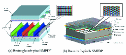
FIGURE 1 — Panel structure of an SMPDP.
Discharge characteristics of a new ACPDP structure using Thick-Film Ceramic Sheet technology
Naoya Kikuchi
Shinsuke Mori
Hideyuki Asai
Noritake Co., Ltd.
Abstract — A counterelectrode PDP structure in which the sustain and scan electrodes are embedded face to face in the ribs by applying Thick-Film Ceramic Sheet technology is proposed. An advantage of the counterelectrode PDP is low discharge voltage, which does not depend on the dielectric thickness. A positive column is observed at a longer gap, and the luminous efficacy reaches 3.7 lm/W at Ne–30%Xe at a 450-μm discharge gap.
This counterelectrode PDP should have several advantages as follows:
1. All the electrodes are placed on a front plate. 1.1 ITO electrode is not necessary.
1.2 The dielectric layer should not necessarily be transparent.
1.3 The protective layer also should not necessarily be transparent.
2. There is greater flexibility in designing PDP cells.
3. The well-established ADS driving method can be adopted.
TFCS technology has been shown to be appropriate for realizing the counterelectrode PDPs. TFCS can build sustain- and scan-electrode layers that are stacked with the rib layers, making one thick sheet by co-firing both materials. TFCS is independent of a front plate and also a rear plate. Therefore, it is not necessary to control the warping and shrinkage of both plates.
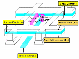
FIGURE 5 — Discharge diagram of the counterelectrode PDP.